
Invented by Richard C. Murphy, Micron Technology Inc
Cache is a temporary storage location that stores frequently accessed data to improve system performance. It acts as a buffer between the processor and the main memory, reducing the time it takes to retrieve data. However, when the data in the main memory is modified, the cache needs to be invalidated to ensure the most recent data is retrieved.
The demand for apparatuses for invalidating cache arises from the need to maintain data consistency and avoid stale or outdated information. In industries such as finance, e-commerce, and real-time analytics, where data accuracy is critical, cache invalidation plays a vital role. Apparatuses for cache invalidation help businesses ensure that their systems are always up to date, providing reliable and accurate information to users.
One of the key drivers of the market for apparatuses for invalidating cache is the increasing adoption of cloud computing. With the rise of cloud-based applications and services, the need for efficient cache management has become even more crucial. Cloud-based systems often handle large amounts of data and require real-time updates, making cache invalidation a critical component.
Furthermore, the growing popularity of mobile applications has also contributed to the demand for cache invalidation apparatuses. Mobile devices often have limited resources, including storage and processing power. Caching frequently accessed data helps improve the performance of mobile applications. However, cache invalidation becomes necessary when the data in the main memory is modified or updated.
The market for apparatuses for invalidating cache is also driven by the increasing complexity of modern software systems. As software becomes more sophisticated and data-intensive, efficient cache management becomes a challenge. Apparatuses for cache invalidation help businesses overcome this challenge by providing automated and efficient ways to invalidate cache.
In terms of market segmentation, the market for apparatuses for invalidating cache can be categorized based on the type of cache being managed. This includes CPU cache, disk cache, and web cache, among others. Each type of cache requires specific apparatuses for efficient management and invalidation.
In conclusion, the market for apparatuses for invalidating cache is witnessing significant growth due to the increasing demand for efficient cache management in various industries. The rise of cloud computing, mobile applications, and complex software systems has further fueled this demand. As businesses strive to provide reliable and accurate information to their users, the need for apparatuses for cache invalidation will continue to grow.
The Micron Technology Inc invention works as follows
The present disclosure comprises apparatuses and methodologies for invalidating cache. A bit vector-capable memory device is an example of a device. It also includes a channel control coupled to the memory. The channel controller can be configured to send a bulk invalidate to a cache memory when a bit vector request is received.
Background for Apparatuses for invalidating cache
Memory devices are usually provided as integrated circuits, or semiconductors, in computer systems. Memory comes in many forms, including volatile and not-volatile. Volatile memory requires power to maintain data (e.g. host data, errors data, etc.). This includes random memory (RAM), DRAM, static random memory (SRAM), SDRAM, and thyristor memory (TRAM), as well as other types of memory. Non-volatile memories can retain data even when they are not powered. They include NAND Flash Memory, NOR Flash Memory, and resistance variable memory. These can be NAND flash, NOR, or resistance variable memory.
Computing systems include many processing resources, such as one or more processors. These can retrieve and execute the instructions, and then store the results in a suitable place. A processing resource (e.g. CPU) can include a number functional units, such as arithmetic unit (ALU), floating point unit circuitry (FPU), and/or combinatorial logic blocks, which are used to execute instructions using logical operators such as AND (and/or), NOT (not and), NAND (or), NOR (or), and XOR (or inversion). Functional unit circuitry can be used, for example, to perform arithmetic functions such as addition, subtractions, multiplications, and/or divides on operands using a variety of logical operations.
Numerous components within a computer system can be involved in the transmission of instructions to functional unit circuitry. Instructions may be carried out by processing resources such as controllers and/or hosts processors. The functional unit circuitry may access a memory array in which data (e.g. the operands that will be used to execute the instructions) is stored. Instructions and/or data can be retrieved from a memory array, and then sequenced or buffered by the functional unit circuitry before it begins to execute instructions. As different types of operation may be performed in one or more clock cycles by the functional unit circuitry it is possible to sequence and/or buffer intermediate results. Operation cycles are a sequence of clock cycles to complete an action. The time required to complete an operations cycle is measured in processing resources, computing performance, and power consumption.
In many cases, the processor (or functional unit circuitry associated with it) is external to the array of memory. Data can be accessed by a bus that connects the processor to the array of memory to execute instructions. In a PIM device, where a processor is implemented internally and/or close to a memory, the processing performance can be improved. PIM devices are defined as devices that have a processor implemented internally and/or close to a memory. A PIM device can save time and power by reducing or eliminating external communication. PIM operations may involve bit vector-based operations. Bit vector operations are performed using contiguous bits, also known as “chunks”. In a virtual address area. A chunk of virtual space, for example, may have a contiguous length of 256 bit. Contiguous virtual address space chunks may or may be physically contiguous.
A typical cache structure (fully associative or set associative) uses a part of the address generated by the processor to determine the location of a data block in the cache. (This is also referred to as a cache block? The cache block may also have metadata (e.g. valid bits and dirty bits) that describe its state. Cache tags are unique identifiers for groups of data stored in the cache. The last-level cache architecture can be based upon 3D integrated memories, where tags and meta data are stored in SRAM on the chip and cache blocks in DRAM that is easily accessed. In this architecture, matching is done using tags stored in SRAM on the chip and memory accesses are accelerated with the DRAM on the package.
A cache architecture can have multiple levels of caching that operate with multiple processor cores. A laptop, for example, may have two processor cores, and two cache levels, one for instructions, and the other for data. The second level cache may also be called the last level cache and can store up to 256 kilobytes. A server can have three or even more cache levels. In a three-level cache, the third level (L3) can be used as the last cache level (LLC). All processing cores must have the same memory view. In order to ensure accurate data access between processing cores, a cache-based memory system uses some form of cache coherent protocol.
Code running on the processing core might want to access an bit vector operation device (e.g. PIM device) to perform a vector-based bit operation. The processing resource of a host generally knows the cache line bit size (a cache block can also be called a cache line). To maintain cache coherency. A bit vector-based operation on a PIM device, however, may use bit vectors with a different bit length. In order to maintain cache coherency, a typical pattern of use for bit vector-based operations in software could involve costly flushing an entire cache and/or marking specific pages as uncacheable. Flushing cache memory is the process of writing an entire cache block back to memory, and then deleting cache entries in order to make space available for the cache memory. Flushing a cache memory can remove useful cache entries and use a lot of power.
By contrast marking invalid cache entries (also known as ‘invalidating’) is a good way to avoid wasting time. “Invalidating” cache entries (also known as ‘cache invalidation’) involves marking specific cache entries, e.g., specific lines in the cache memory. This involves marking certain cache entries (e.g. specific cache lines) and deleting only those cache entries in order to make space available for other purposes within the cache memory. A cache invalidate command that writes a specific entry (e.g. cache line) back to memory, and deletes the cache entry from cache memory to use for another purpose, consumes less time and power than a flushing procedure. Cache invalidation is a technique to ensure that data between a host and memory device is consistent. To make a PIM fully aware of the cache coherency protocols would be costly and complicated.
The present disclosure comprises apparatuses and method for invalidating cache. The embodiments of cache invalidation described herein enable bit vector-based operation requests to be performed on bit vector-operation memory devices, such as a processor in memory (PIM) device. They also allow for more efficient interaction with a memory system cache on a separate device (e.g. a “host”). Processing resource having a bit-vector bit-length that is different from the cache line bit-length. A cache line, for example, in a memory system based on caches, may be 128 bytes (one kilobit), including metadata and tags, along with the cache block data. A bit vector operation device, such as a PIM device, can operate on data blocks in “chunks”. The bit width may be equal to the block width of a DRAM or a selected bit width, depending on the design implementation. In one embodiment, a chunk can be selected to have a 256-bit bit width to match the width of an interface bandwidth. In a cache-based memory system, four (4) pieces may equal a total cache line bit size of 128 bytes.
As used in this document, the term “bit vector” is intended to mean a physically contiguous number of bits. It is meant to refer to a number of physically contiguous bits. Physically contiguous bits can be stored on a bit-vector memory device (e.g. PIM) whether they are physically contiguous horizontally or vertically in an array. A ‘bit vector operation’ is used in this document. As used herein, a?bit vector operation? Virtual address space is used, for example, by PIM devices. “A chunk can be physically contiguous or not to other chunks within the virtual address space.
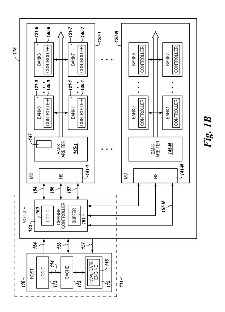
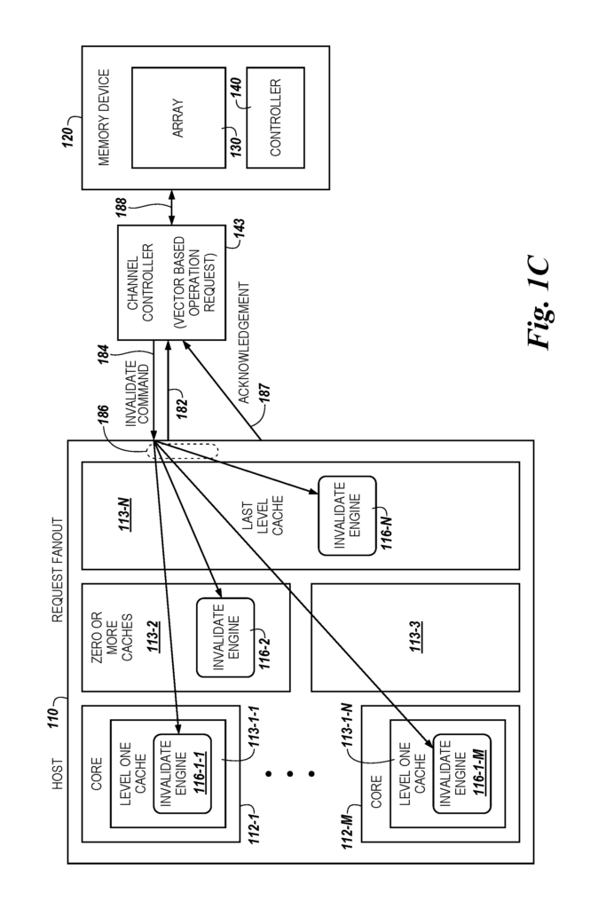
In an example embodiment, a device comprises a memory cell array and sensing circuitry connected to the array. The sensing circuitry consists of a sense amplifier, and a compute element configured to perform logical operations. A memory controller coupled to the array of sensing circuitry is configured to receive an operation request for bit vectors. A channel controller coupled to the memory device is configured to send a bulk invalidate to a cache system in response to receiving a bit vector request. In the context of this document, a cache-based memory system is also referred to as a “cache memory system”. This term is used to refer to an apparatus (e.g. component, device or system) that is associated with a specific cache coherency protocols. The term “bulk invalidate” is used in this document. This is meant to be a capability that allows you to address multiple locations and invalidate the information, e.g. multiple cache lines without having to individually address and communicate invalidate instruction to each location. As previously mentioned, marking entries in a cache as invalid (also known as “invalidating”) is a common practice. As mentioned above, invalidating cache entries (also known as ‘invalidating? The deletion of the contents from a cache entry is used to release space in the cache memory. In certain embodiments, a cache invalidate operation is used to free up memory space for operations performed on a PIM.
In the detailed description that follows, the drawings are referred to as they form part of this disclosure and show how certain embodiments can be implemented. The embodiments described herein are sufficiently detailed to allow those with ordinary skill to perform the disclosure. However, it should be noted that other embodiments can be used and that electrical, structural, or process changes may be made, without departing the scope of this disclosure. When used in this document, designators like?N? or?M’, especially with reference to the numerals of the drawings, indicate a number that can be included. ‘A number of’ is used in the following. A particular thing may refer to more than one of these things (e.g. a number memory arrays could refer to more than one memory array). A ‘plurality of’ “This phrase is meant to include more than one such thing.
The figures in this document follow a numbering scheme in which the first or second digit corresponds to the drawing figure and the remainder of the digits identify a component or element in the drawing. Similar digits can be used to identify similar elements or components in different figures. 206 could refer to element?06′. In FIG. In FIG. 6. It will be understood that elements in the embodiments shown here can be substituted, removed, or added to create a variety of other embodiments. As will also be appreciated, both the relative size and proportion of the elements in the figures were chosen to illustrate specific embodiments of the invention and not as a limitation.
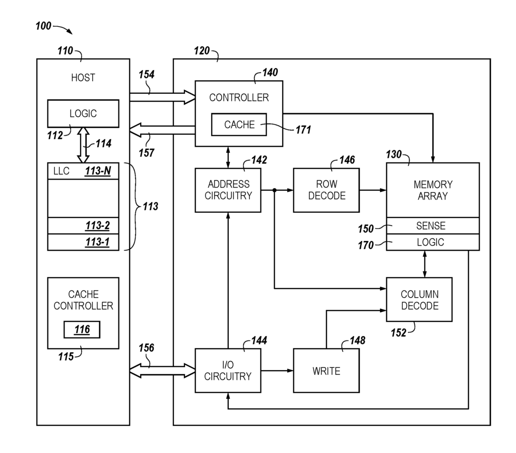
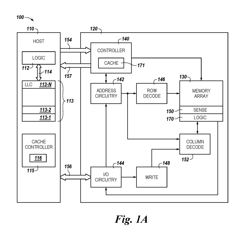
FIG. Block diagram 1A shows an apparatus that is a computer system with a memory device, according to a variety of embodiments. As shown in FIG. As shown in FIG. As used in this document, logic can refer to hardware such as transistors and/or ASICs and firmware. In at least one embodiment, the logic resources 112 may include a static random-access memory (SRAM) on the logic resources 112 (also referred to sometimes as a “logic layer”). In the embodiment shown in FIG. The logic resource 112 on the host can be coupled to the cache memory 113, such as in 3D integrated memories, via a wide interface 114, also referred to on-chip or on-die. The logic component 112 may be coupled to the host memory 113 through a wide interface, such as a 256-bit interface. This interface can include through silicon vias as part of a 3-D integrated memory with multiple memory die stacked onto a logic die.
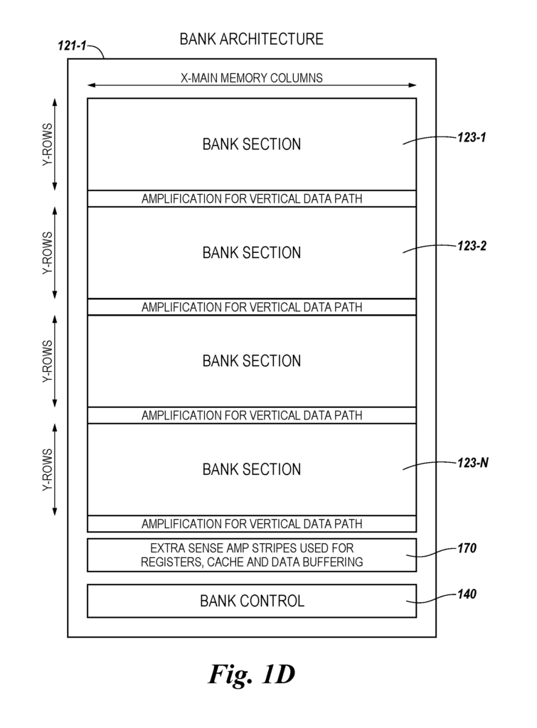
In one or several embodiments, the cache memory can have a number of cache levels. 113-1, 113-2, . . . Embodiments do not limit themselves to 113-N. In at least some embodiments, a portion may be used as a level (level) of a cache memory (LLC), such as 113-N. This structure allows the LLC 113N to control the block data alignment. As will be apparent from this description, an overall size of the cache memory of a 3D or logic integrated memory chip can be reduced.
As shown in FIG. In 1A, a cache control 115 can be provided. This controller may include logic, such as firmware, hardware (e.g. an ASIC), or software, which includes instructions stored in memory that are executed by the logic resource 112 and/or logic. In some embodiments, the firmware or software of the cache controller 115 may include an invalidate algorithm 116 that is associated with the cache coherency protocol for the cache memory 113. In certain embodiments, the caching controller 115 can be configured to execute instructions or perform logic operations to maintain a coherency protocol associated with cache blocks (also known as cache lines?) The cache memory 113 contains a cache coherency protocol. A cache coherency may be a MESI protocol (modified exclusive shared invalid), or a directory based cache protocol, etc. These examples are only examples. Cache line (?cache blocks?) is used in this context. The term “cache line” (?cache block?) is used herein to refer to a basic unit of storage for the cache and can contain multiple words/bytes of data. In some embodiments, the cache controller can add metadata such as subrow select metadata or block select metadata to a line of cache. Block select metadata, for example, may enable an offset in the cache line. Subrow select metadata can enable multiple sets within a set-associative cache. In one embodiment, the block select metadata provides an offset for a page within a dynamic random-access memory (DRAM).
In order to understand improved system operation techniques and the apparatus for implementing them, we will discuss a bit-vector operation memory device (e.g. PIM device) and its associated host. In various embodiments instructions, such as PIM commands (microcodes), can be sent from a host to a memory having PIM capabilities in order to perform logical operations. The PIM device can store PIM commands in a memory array, and the controller of the memory device can execute the commands without having to send commands back and fourth over a network. PIM commands can be executed by the memory device in order to perform logical functions on the device. This may take less time and use less power than performing the same function on the host. Reduced data movement within a computer system can also result in time and energy savings.
Numerous embodiments of the disclosure can provide better parallelism or reduced power consumption when performing compute functions compared to prior systems, such as PIM systems, and systems with an external processor. (e.g. a processing resource external from a storage array, such as located on a separate integrated chip). As an example, certain embodiments allow for the performance of fully-complete compute functions, such as integer addition, subtraction, multiplying, dividing, and CAM functions (content addressable memories), without having to transfer data from the memory array or sensing circuitry through a bus. These compute functions may involve a variety of logical operations, such as AND/OR, NOT/NOR, NAND/XOR, XOR etc. The embodiments of the invention are not limited to this example. “For example, performing logical operation can include performing non-Boolean operations such as copying, comparing, destroying, etc.
In prior approaches, data can be transferred (e.g. via a bus containing input/output (I/O), lines) from an array and sensing to a computing resource, such as a microprocessor or compute engine. This processing resource may include ALU circuitry, and/or functional unit circuitry, configured to perform the necessary logical operations. Transferring data from a sensing and memory array to such processing resources can consume significant power. Even if the computing resource is on the same chip as the memory, it can consume significant power in moving data from the array to compute circuitry. This can include performing a sense-line (which can be referred here as a data line or a digit-line) address access (e.g. firing a column decoder signal) to transfer data.
Furthermore the circuitry in the processing resources (e.g. compute engine) might not comply with pitch rules associated to a memory array. As an example, the memory array cells may be 4F2 or even 6F2 in size. The feature size for the cells is “F”. The devices (e.g. logic gates) that were associated with ALUs in previous PIM systems might not be able to be formed on pitch, which could affect chip size or memory density. “A number of embodiments in the present disclosure have sensing circuitry that is formed on pitch along with an array memory cells, and can perform compute functions.
Again, FIG. The block diagram 1A shows an apparatus consisting of a computer system 100 with a memory device, according to a variety of embodiments. Above, we have discussed the host 110 and its logic resource 112, as well as cache memory 113. The memory device shown in FIG. 1A may include a controller memory 140, a sensor circuitry 150 or logic circuitry 170. As used here, each of these could also be considered separately as an “apparatus.
Click here to view the patent on Google Patents.
Leave a Reply