
Invented by Hae Yeon Hwang, Yung Ho Ryu, Da Mi Shim, Se Hwan Ahn, Samsung Electronics Co Ltd
Vertically arranged LEDs are designed to emit light in a vertical direction, providing better light output and efficiency compared to their horizontal counterparts. This unique design allows for improved heat dissipation, resulting in longer lifespan and reduced energy consumption. Additionally, vertically arranged LEDs offer enhanced brightness and color uniformity, making them ideal for applications that require high-quality lighting, such as displays, signage, and automotive lighting.
One of the key drivers of the market for vertically arranged LEDs is the growing demand for energy-efficient lighting solutions. As governments and organizations worldwide focus on reducing energy consumption and carbon emissions, LED technology has emerged as a viable alternative to traditional lighting sources. The vertical arrangement of LEDs further enhances their energy efficiency, making them an attractive option for both residential and commercial lighting applications.
Another significant factor contributing to the market growth is the increasing adoption of LED displays in various industries. Vertically arranged LEDs are particularly well-suited for large-scale displays, such as video walls and outdoor billboards. Their improved brightness and color uniformity ensure vibrant and eye-catching visuals, making them popular in advertising, entertainment, and sports industries.
Furthermore, the automotive industry is witnessing a surge in the use of vertically arranged LEDs for lighting applications. These LEDs offer superior performance in terms of brightness, energy efficiency, and design flexibility, making them an ideal choice for headlights, taillights, and interior lighting. The demand for advanced lighting solutions in the automotive sector, coupled with the growing trend of electric vehicles, is expected to drive the market for vertically arranged LEDs in the coming years.
In terms of geographical distribution, the market for vertically arranged LEDs is witnessing significant growth in Asia Pacific, particularly in countries like China, Japan, and South Korea. These countries are major manufacturing hubs for LED products and have a strong presence in the global electronics industry. The increasing investments in research and development activities, coupled with favorable government initiatives promoting energy-efficient lighting solutions, are driving the market growth in this region.
Overall, the market for the method of manufacturing vertically arranged LEDs is poised for substantial growth in the coming years. The advantages offered by this technology, including improved energy efficiency, enhanced brightness, and design flexibility, make it a preferred choice in various industries. As the demand for energy-efficient lighting and advanced display solutions continues to rise, the market for vertically arranged LEDs is expected to expand further, presenting lucrative opportunities for manufacturers and suppliers in the global market.
The Samsung Electronics Co Ltd invention works as follows
A method is described for the manufacture of a vertically-structured LED that can be separated with ease. The method involves forming a light emitting structure on a growth surface with a plurality device regions, and at least one isolation region. This light-emitting layer has a n-type layer, an activated layer, and a P-type layer, which are all arranged on the growth surface in sequence. On the light-emitting substrate, a p-electrode can be formed. On the p electrode, a plating layer connects all the device isolation regions. On the first plating of the device area, a pattern of a secondary plating is formed. The growth substrate of the device region is removed and an n electrode is formed on the n type clad layers.
Background for Method of manufacturing vertically arranged light emitting diode
1. “1.
The present invention is a new method of manufacturing a light emitting diode with a vertical structure that allows for easy chip separation for each element.
2. “2.
A gallium-nitride-based semiconductor is AlxGayIn1x?yN (0xGayIn1x?yN, 0xGayIn1x?yN, 0x+y+y?1) is a compound semiconducting material that is adaptive to light-emitting at ultraviolet wavelengths and is used in a green or blue light emitting diode. GaN LEDs are classified into two main types: a horizontally-structured GaN LED and a vertically-structured GaN LED. The horizontally-structured GaN-based device has both an n and a p electrode on the same side. The LED device’s total surface area should be large to ensure a sufficient amount of light emission. The horizontal GaN-based LED can be vulnerable to ESD because the transparent electrode and n-electrodes are so close together.
The vertically-structured GaN LED, on the other hand, has a number of advantages over the horizontally-structured GaN LED. The n-electrode is disposed in the middle of the GaN-based vertically-structured LED.
Typically, vertically-structured GaN-based leds are manufactured by attaching a conductive surface (e.g. a silicon substrate or a Gallium Arsenide (GaAs), and then removing a growth surface (e.g. a sapphire). Korean Patent Laid Open Publication No. “2004-58479 discloses the manufacturing of vertically-structured GaN-based LEDs, including an attachment of a Si substratum, a removal of a sapphire substratum, and a cutting process of the Si Substratum.
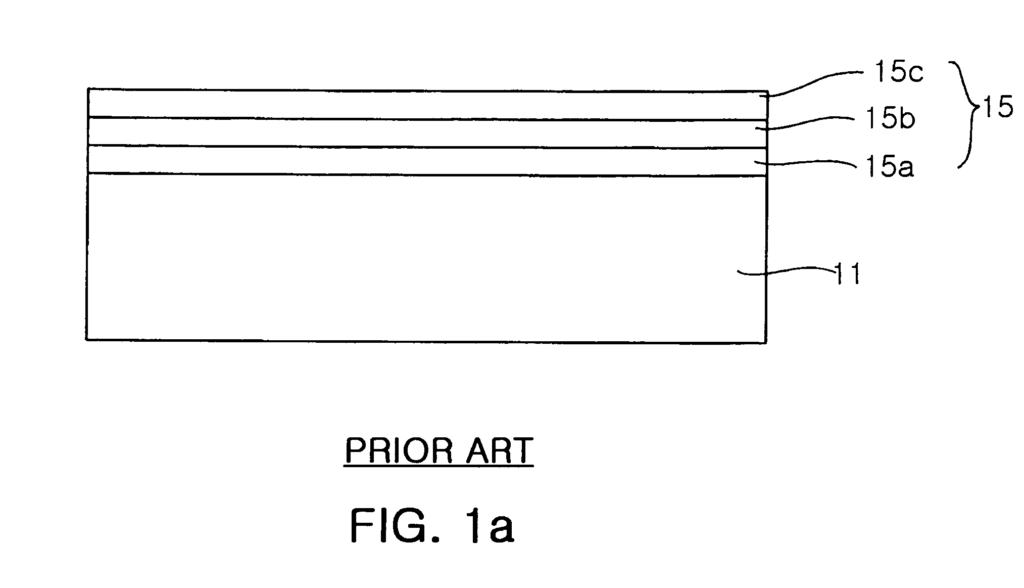
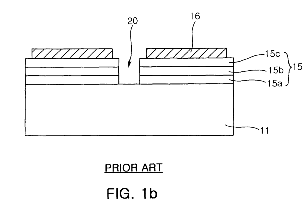
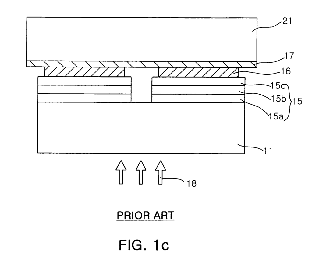
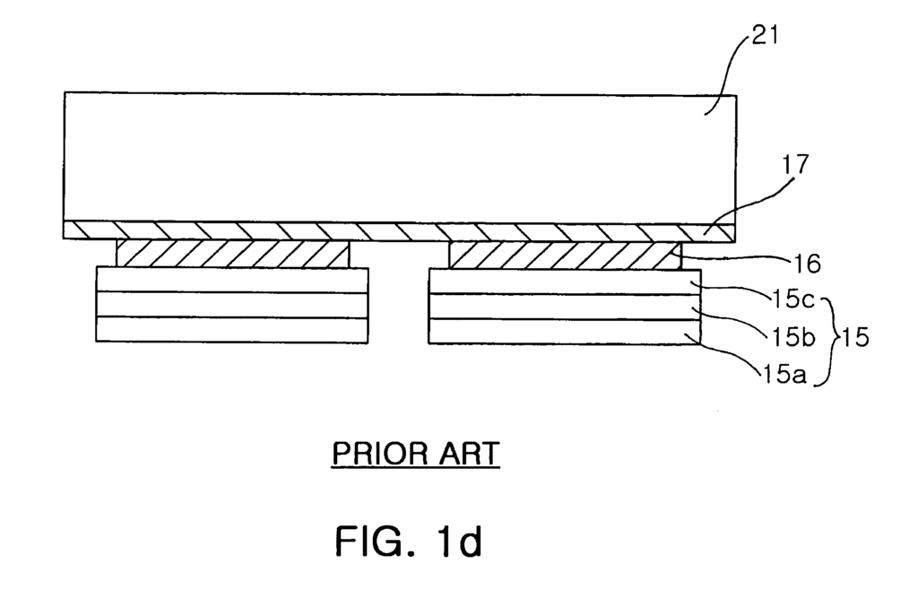
FIGS. The cross-sectional views 1A to 1F illustrate a conventional manufacturing method for a vertically-structured GaN-based led. Referring to FIG. On a sapphire surface 11, an n-type clad 15 a, a GaN-based active layer 15b, and a p type clad 15c are sequentially deposited. Referring to FIG. Referring to FIG. A conductive substrate 21, such as a Si or GaAs substrate or similar, is attached to the p electrode 16 by using a conductive glue layer 17, such as gold or other metals. The sapphire substrate is then removed from the light emitting structure 15 using a laser lift-off procedure. A laser beam 18 is focused on the sapphire 11 to remove the sapphire 11 from the light emitting structure 15. As a result, the structure is formed where the sapphire 11 has been removed as shown in FIG. 1D. Referring to FIG. On the n type clad layer 15, a n-electrode is formed. Referring to FIG. The resultant structure from FIG. “1E is separated into individual elements by chip separation, resulting in a multitude of GaN-based LEDs with vertically structured structures 10 at the same time.
According to the conventional method of separating the chips, it is necessary to cut away the conductive surface 21. To cut away the conductive surface 21, use a cutting wheel to perform a dicing procedure. A more complicated process, such as the scribing-and-breaking process, is required. Due to the complexity of the process, manufacturing costs are increased, and the overall process time is subsequently delayed. The thermal conductivity is low in the Si or GaAs substrates used as conductive substrates 21. This results in a poor heat release efficiency and deterioration of device characteristics when high currents are applied. The device can be damaged if a crack occurs in the light emitting structure 15 when attaching the conductive surface to it. This problem can also occur during the production of LEDs with vertically-structured structures using other compound semiconductors in group III-V. For example, vertically-structured AlGaInP LEDs, AlGaAs LEDs, or similar devices.
The present invention is directed at a method of manufacturing a vertically-structured light emitting device that eliminates one or more problems caused by limitations and disadvantages in the related art.
The present invention aims to create a light-emitting LED with a vertical structure that can easily perform a chip separation and improve the efficiency of heat dissipation.
The description of the invention includes additional advantages, features, and objects. These will be revealed in part by the description that follows, while others will be apparent to anyone with ordinary knowledge of the art after reading the description or from the practice of the invention. The written description, claims and drawings of the invention will show how the objectives and other benefits can be achieved.
The present invention provides a method of manufacturing a vertically-structured light-emitting device (LED), which includes the steps of: forming the p electrode on the light emitting structure, forming the first plating on the p electrode to connect the plurality device regions, forming the pattern of a 2nd plating on the 1st plating of the device region; removing the growth layer and forming the n electrode on top of the n type clad.
According to another aspect, the method includes, before the formation of the first plating, forming a slit in an area of light-emitting structures on the device isolation regions, to separate each device region.
According to a further aspect of the invention, the method includes: After removing the growth medium, forming an area of light-emitting structures on the device isolation regions, to separate each device region.
Preferably the method further comprises: after forming a trench, forming an additional passivation layer over a side of the light emitting structure that is divided into individual device regions.
According to a further aspect of the invention, after forming an n-electrode the method includes removing the first layer of plating of the device isolating region by wet cleaning. The first plating is preferably formed from a different metallic material than that of the secondary plating, and has a greater etch selectivity.
According to a further aspect of the invention, after forming the n electrode, the method includes breaking away the first layer of plating of the device’s isolation region.
According to a further aspect of the invention, after forming the n electrode, the method includes cutting away the first layer of plating of the device separation region by irradiating the laser beam onto the first layer formed over device isolation area. The laser cutting of the plating layer allows for the separation of individual chips without the need to perform additional dicing and scribing processes.
The first plating layer can be made of at least one metal material from the following group: Au, Cu Ni Ag Cr W Al Pt Sn Pb Fe Ti Mo and any combination of these materials. The second plating can be made of any metallic material from Au, Cu Ni Ag Cr W Al Pt Sn Pb Fe Ti Mo.
According to a further aspect of the invention, the first layer of plating is coated over the entire surface, including the top surface the p-electrode. The first plating is also formed so that it exposes a portion the device isolation area.
Accordingly, a further aspect of the invention is that the step of forming a first plating layer consists of: forming?a seed for plating? The p-electrode is positioned so that it connects a plurality of device areas. The seed layer can be formed using an electroless plating process or by deposition.
Click here to view the patent on Google Patents.
Leave a Reply