Invented by Nobuyuki HATANAKA, Tadahiro Kobayashi, Akira Yokota, Sumitomo Chemical Co Ltd
One of the key drivers of the market for the method of producing laminated bodies is the increasing demand for lightweight and fuel-efficient vehicles. Laminated bodies offer several advantages over traditional metal structures, including reduced weight, improved strength, and better resistance to corrosion. This has led to their widespread adoption in the automotive industry, where manufacturers are constantly striving to meet stringent fuel efficiency standards.
Moreover, the aerospace industry has also embraced the use of laminated bodies due to their high strength-to-weight ratio. The lightweight nature of laminated bodies allows for increased payload capacity and improved fuel efficiency in aircraft. Additionally, laminated bodies offer better resistance to fatigue and impact, making them ideal for use in critical components such as wings and fuselages.
In the construction industry, laminated bodies are used in the production of doors, windows, and other structural elements. The ability to combine different materials in the lamination process allows for the creation of products with enhanced thermal and acoustic insulation properties. This has led to increased demand for laminated bodies in the construction sector, where energy efficiency and sustainability are key considerations.
Furthermore, the electronics industry has also witnessed a surge in the use of laminated bodies. These bodies are used in the production of printed circuit boards (PCBs) and semiconductor devices. Laminated PCBs offer improved electrical performance, reduced signal loss, and enhanced reliability. With the growing demand for smaller and more powerful electronic devices, the market for laminated bodies in the electronics industry is expected to expand further.
In terms of geographical distribution, the market for the method of producing laminated bodies is dominated by North America and Europe. These regions are home to several major automotive and aerospace manufacturers who have been early adopters of laminated body technology. However, emerging economies in Asia Pacific, such as China and India, are also witnessing rapid growth in this market. The increasing industrialization and urbanization in these countries are driving the demand for laminated bodies in various sectors.
In conclusion, the market for the method of producing laminated bodies is experiencing robust growth due to the numerous advantages offered by this technology. The automotive, aerospace, construction, and electronics industries are the major contributors to this market. With the increasing focus on lightweight and sustainable materials, the demand for laminated bodies is expected to continue rising in the coming years.
The Sumitomo Chemical Co Ltd invention works as follows
Method for making a thin optically laminated body. This method is for producing a thin optical laminated body that includes a polarization, a negative C, and a polarization, as well as a polarization, a negative C, and a polarization, in the order described by the member; the positive C between the two layers, or on the opposite side of the layer arranged with the polarization, or the side of a polarization, and the negative C; and the transfer adhesion layer between these two layers or the polarization, a
Background for Method of producing laminated body
Field of Invention
The present invention is a method of producing a laminated structure.
Description of Related Art
International publication No. WO 2003/100115 describes circularly polarizing plates that include a /4 layer, an /2 layer, and a layer of polarization.
When the organic EL displays show a black screen, there may be light leakage in the oblique field of view.
The present invention is described as follows:
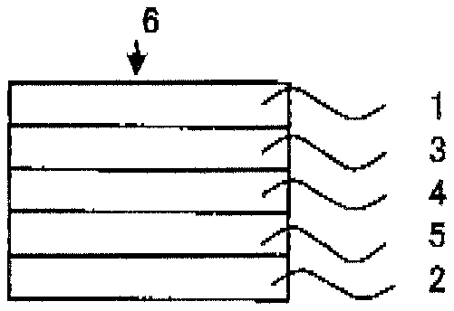
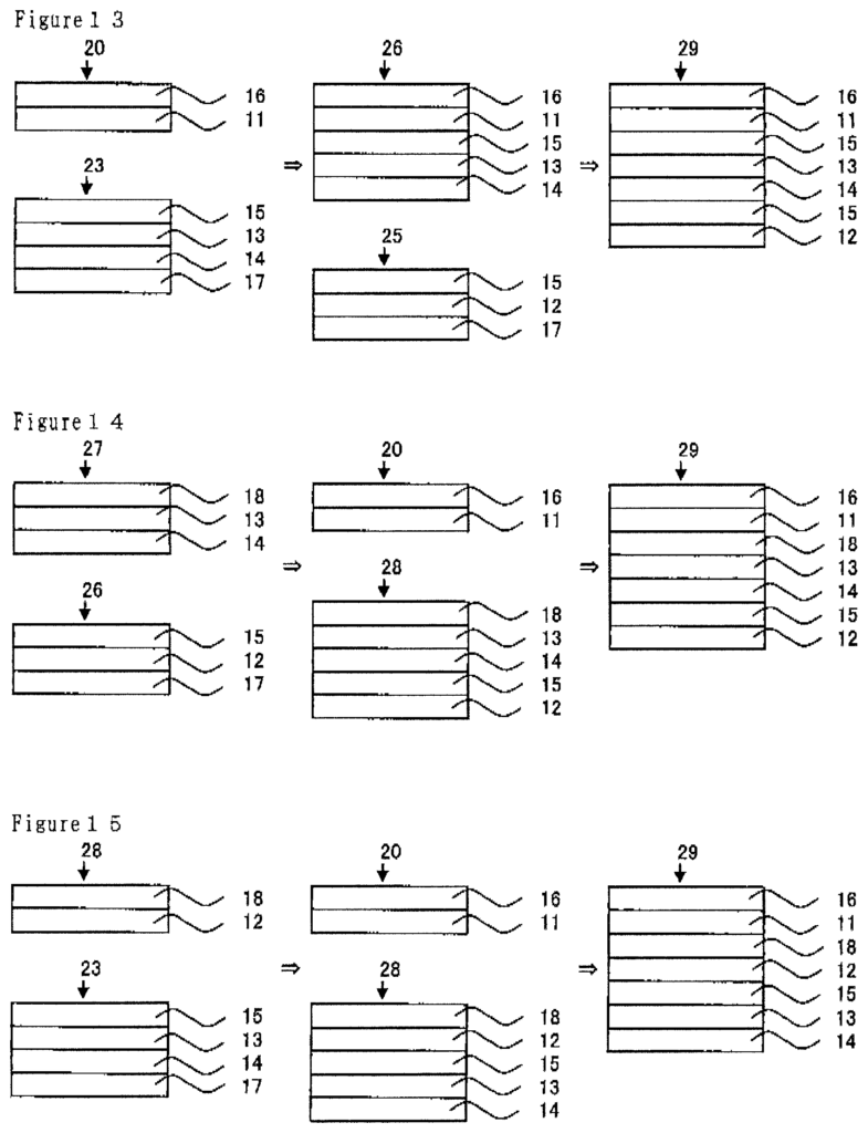
[1] A process for producing a laminated material including a polarization, a negative C, a /2, a 44 layer and a transfer adhesive;
the laminated structure is a laminated structure:
including the polarization layers, the /2 layer and the >/4 layer in the member-described orders,
including the positive layer C between the polarization and the /4 layer or on the opposite side of the layer /4 to that of the arranged?/2 layer; and
including the transfer adhesion layer between the polarization layers, and the positive C layer or?/4 layer; and
The method includes the steps of adhering a bonding layer including a substrate, the transfer adhesive and an adherend to the transfer layer and peeling off the substrate.
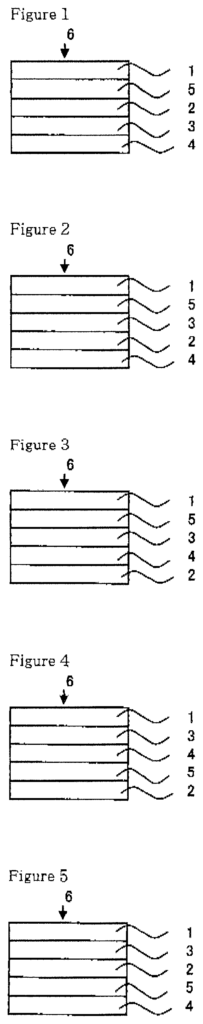
[2] A method for producing a laminated body that includes the polarization, transfer adhesive, positive C,?/2, and?/4 layers in the member-described sequence;
The bonding body being
a ready-prepared laminated body including the transfer adhesion layer, the positive C layers, and the substrate, in this member-described ordering,
a ready-prepared laminated body including the transfer adhesion layer, positive C layer and the?/2 layers in this member-described ordering, or
a ready-prepared laminated body comprising the transfer adhesive layer (positive C), the?/2 and?/4 layers, and the substrate, in the order described by the member;
the adhernd being an adhesivend including the polarization layers; and
the method includes the step of adhering the bonding body side outer surface to the polarization layers side outer surfaces of the adherend by bonding through the transfer glue layer and peeling off the substrate.
[3] A method for producing a laminated body that includes the polarization and transfer adhesive layers, as well as the?/2, positive C,?/4, and?/4 layers in the member-defined order;
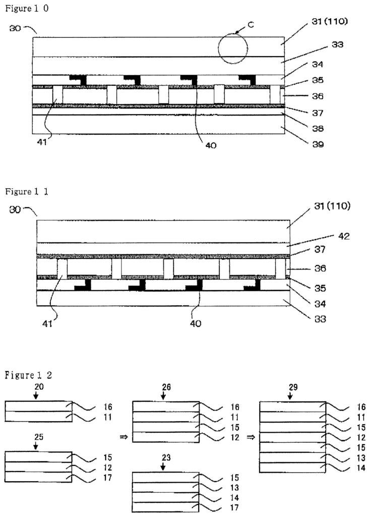
The bonding body being
Click here to view the patent on Google Patents.
Leave a Reply