
Invented by Sang Won Kang, Yong Chun Kim, Dong Hyun Cho, Jeong Tak Oh, Dong Joon Kim, Samsung Electronics Co Ltd
Nitride semiconductor light-emitting devices have revolutionized the lighting industry with their energy-efficient and long-lasting properties. These devices, which include light-emitting diodes (LEDs) and laser diodes, have become increasingly popular in various applications such as general lighting, automotive lighting, and displays. The global market for nitride semiconductor light-emitting devices is expected to witness significant growth in the coming years, driven by advancements in fabrication methods and increasing demand for energy-efficient lighting solutions.
One of the key factors driving the market for nitride semiconductor light-emitting devices is their superior performance compared to traditional lighting technologies. Nitride semiconductors, such as gallium nitride (GaN), have a wide bandgap, allowing for the emission of light in the visible spectrum. This property enables the production of LEDs with high brightness and color purity, making them ideal for applications that require high-quality lighting, such as outdoor and indoor lighting, automotive headlights, and displays.
Moreover, nitride semiconductor light-emitting devices offer several advantages over traditional lighting technologies. They have a longer lifespan, consuming significantly less energy and requiring fewer replacements, thus reducing maintenance costs. Additionally, they are more environmentally friendly as they do not contain hazardous materials like mercury, which is commonly found in fluorescent lamps. These benefits have led to a growing adoption of nitride semiconductor light-emitting devices in both residential and commercial sectors, driving the market growth.
The method of fabrication plays a crucial role in the performance and cost-effectiveness of nitride semiconductor light-emitting devices. Over the years, significant advancements have been made in the fabrication techniques, leading to improved device efficiency and reduced production costs. One of the key fabrication methods is metal-organic chemical vapor deposition (MOCVD), which allows for the precise control of material composition and thickness, resulting in high-quality nitride semiconductor layers. MOCVD has become the preferred method for large-scale production of nitride semiconductor light-emitting devices due to its scalability and cost-effectiveness.
Another promising fabrication method is the epitaxial lateral overgrowth (ELO) technique, which enables the growth of nitride semiconductor layers with reduced defects and improved crystal quality. This technique has the potential to further enhance the performance of nitride semiconductor light-emitting devices, making them more efficient and reliable.
The market for nitride semiconductor light-emitting devices is highly competitive, with several key players dominating the industry. Companies such as Nichia Corporation, Cree Inc., and Osram Opto Semiconductors GmbH are at the forefront of innovation, continuously developing new products and improving fabrication techniques. These companies invest heavily in research and development to stay ahead of the competition and meet the evolving demands of the market.
In conclusion, the market for nitride semiconductor light-emitting devices is witnessing significant growth due to their superior performance, energy efficiency, and environmental friendliness. The advancements in fabrication methods, such as MOCVD and ELO, have further fueled the market growth by improving device efficiency and reducing production costs. As the demand for energy-efficient lighting solutions continues to rise, the market for nitride semiconductor light-emitting devices is expected to expand further, offering immense opportunities for manufacturers and investors in the coming years.
The Samsung Electronics Co Ltd invention works as follows
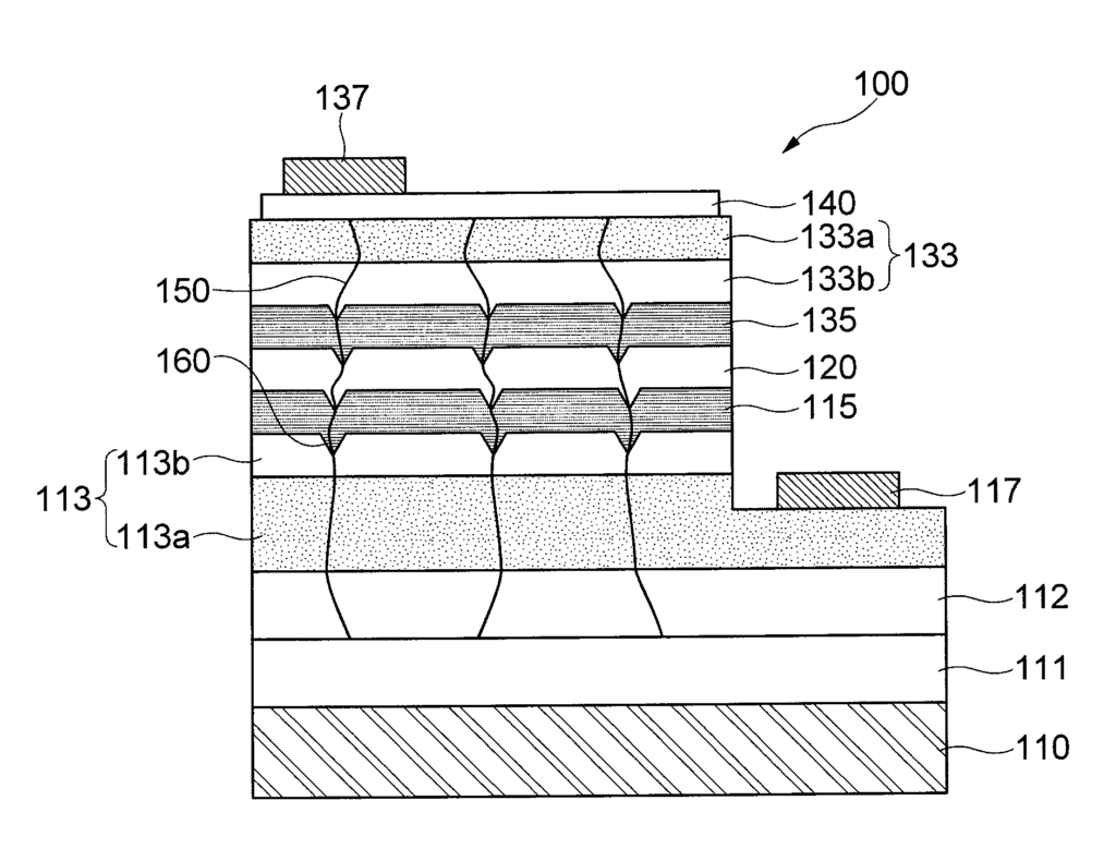
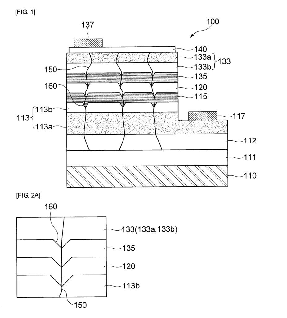
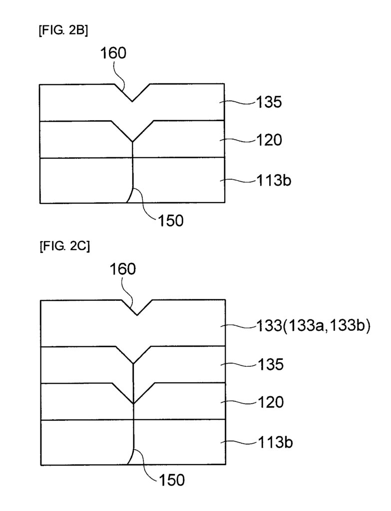
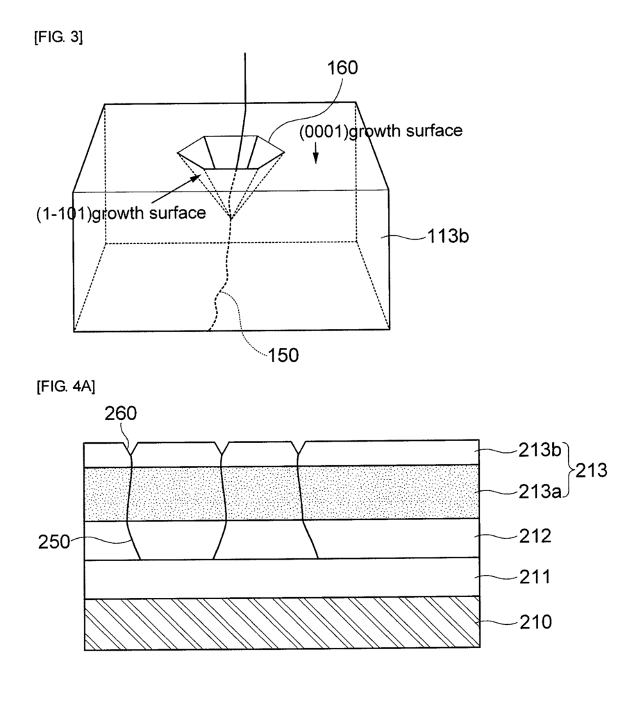
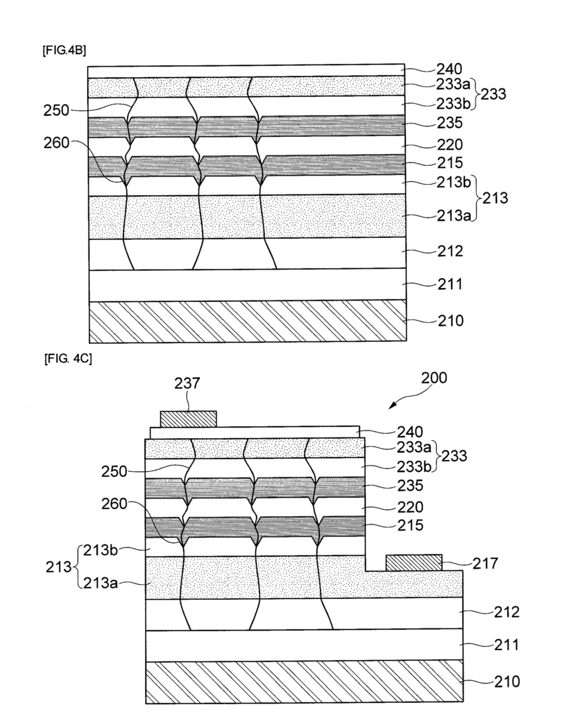
The present invention is a GaN-based nitride-based light-emitting device with improved Electrostatic Discharge (ESD), tolerance (withstanding properties), and a fabrication method including a substrate, a V-shaped distortion made up of an n type nitride layer, an active and a p type nitride layer on the substrate. This structure was formed by referring to the n type nitride layer.
Background for Nitride Semiconductor Light-Emitting Device and Method of Fabrication Thereof
1. “1.
The present invention is a nitride-based semiconductor light-emitting device, and more specifically, a nitride-based semiconductor light-emitting device that can improve the ESD (Electrostatic discharge) tolerance (withstand voltage characteristics) of a GaN base nitride device, and a manufacturing method.
2. “2.
This is because a lot of crystal defects are formed in a GaN thin film due to a great lattice mismatch (16%) between a substrate and a thin film to be grown since the GaN light emitting device is formed on a sapphire substrate having a great lattice mismatch. The reason for this is because a large number of crystal defects form in a GaN film due to the great lattice difference (16%) between the substrate and thin film that is to be formed, since a GaN light-emitting device is grown on sapphire substrates with a high lattice difference.
This crystal defect increases the leakage current and an active surface of a light-emitting device with many crystal defects will be broken when external static electricity is used. It is generally known that crystal defects (threading displacements) of the order 1010-1012/cm2 are present at the GaN film.
The static electricity breaking characteristic of the GaN-based light emitting devices is an important issue in relation to their application range. A design for devices that can withstand static electricity generated by package devices and workers is an important parameter to improve the yield of a final product.
The static electricity characteristic is becoming more important, especially since GaN-based light emitting devices are being used in a poor environment like an outdoor signboard or a vehicle lamp.
In general, the ESD (Electrostatic discharge) of a GaN light-emitting device can withstand thousands of volts when used in HBM (Human Body Mode), but not in reverse. As described above, the electrode design and crystal defects are the main reasons. The GaN light-emitting device, which uses sapphire as an insulator in most cases, has an ESD characteristic that is further degraded when currents are concentrated around the N-electrode. This occurs because the P-electrode, as well as the N electrode, are located on the same plane of the device structure.
A conventional method of improving ESD characteristics has often been approached on the external aspects of devices. U.S. Pat. No. No. 6,593,597 describes a method for protecting an ESD-sensitive light emitting device by connecting a Schottky and LED in parallel, by integrating both the LED and Schottky on the same substrate. A method of connecting an LED and a Zenor Diode in parallel was also proposed to improve ESD tolerance. These methods are less desirable in terms of cost and yield because they require additional Zenor diodes or a Schottky connection, which increases the cost to manufacture the device.
The most preferred method is to improve the ESD characteristics of the light-emitting device itself, by improving the thin-film characteristic or the structure of the device. Japanese Pat. No. No. No. No. 3,063,756, Japanese Patent No. No. 3,424,629 Japanese Patent No. No. 2006-237254, U.S. Pat. No. No.
The ESD characteristics of GaN have been improved by using a growing method for thin films.
The present invention was invented to overcome these problems. It is therefore an object of this invention to provide a semiconductor nitride light emitting device, and a fabrication technique thereof, capable of improving the ESD effect through changing factors to reduce leakage by using crystal defects in the opposite direction (threading dislocations), which were the reason for conventional leakage.
The present invention is a nitride-semiconductor light-emitting device that includes a substrate, a light-emitting structure consisting of an n type nitride-semiconductor layer, an active-layer and a P-type-nitride-semiconductor layer sequentially formed on the substrate, with threading-dislocations piercing the n-type-nitride-s
And the substrate can be selected from sapphire (MgA1204) substrates, ZnO substrates, GaAs substrates, GaN, SiC substrates, and spinel substrates.
The nitride-based semiconductor light emitting devices further include a buffer between the substrate, and the n type semiconductor layer. It is preferred that the buffer is made of either a nitride-based semiconductor or a carbide-based semiconductor.
The n-type GaN-based semiconductor layer is composed of an n type super lattice and an n type GaN-based semiconductor layer.
The super-lattice layer is constructed using a multi-stacked AlGaN/GaN/InGaN structure. An n type electrode can then be added to the GaN-based semiconductor.
And it is preferred that the V-shaped distorting layer is formed on the surface of the GaN-based n-type Nitride semiconductor layer.
The active layer can be built with InGaN/GaN.
The p type nitride based semiconductor layer is constructed using a p type super lattice and an AlGaN/GaN/InGaN multi-stacked structure.
A transparent electrode and a binding electrode are also included on the p type nitride nitride layer.
Click here to view the patent on Google Patents.
Leave a Reply