
Invented by Dong Soo Choi, Jin Woo Park, Samsung Display Co Ltd
One of the key advantages of OLED displays is their ability to produce vibrant and high-quality images. Unlike LCD displays that require a backlight, OLED displays emit light directly from each pixel, resulting in deeper blacks, wider viewing angles, and more accurate color reproduction. This feature makes OLED displays particularly suitable for applications where image quality is crucial, such as in high-end smartphones and televisions.
Another significant advantage of OLED technology is its flexibility. OLED displays can be made on flexible substrates, allowing for the creation of curved or even rollable displays. This flexibility opens up new possibilities for design and form factor, enabling manufacturers to create innovative and unique products. For instance, curved OLED displays have been widely adopted in smartphones, providing a more immersive viewing experience.
Energy efficiency is also a key factor driving the demand for OLED displays. Since OLEDs emit light directly, they do not require a separate backlight, resulting in lower power consumption compared to LCD displays. This energy efficiency is particularly important for portable devices, such as smartphones and wearable devices, where battery life is a critical factor.
The market for OLED displays is expected to witness significant growth in the coming years. According to a report by Market Research Future, the global OLED market is projected to reach a value of USD 48.81 billion by 2023, growing at a CAGR of 14.7% during the forecast period. The increasing adoption of OLED displays in smartphones, televisions, and automotive displays is expected to drive this growth.
Smartphones are one of the largest contributors to the OLED market. The demand for smartphones with OLED displays has been steadily increasing due to their superior image quality and energy efficiency. Major smartphone manufacturers, such as Apple and Samsung, have already incorporated OLED displays in their flagship devices, further boosting the market growth.
The television industry is also witnessing a shift towards OLED technology. OLED TVs offer an unparalleled viewing experience with their deep blacks, vibrant colors, and wide viewing angles. As the prices of OLED TVs continue to decline, more consumers are opting for OLED TVs over traditional LCD TVs, driving the market growth.
Furthermore, the automotive industry is also embracing OLED displays for their infotainment systems and instrument clusters. OLED displays provide better visibility under different lighting conditions and can be integrated seamlessly into the vehicle’s interior design. The increasing demand for connected and electric vehicles is expected to further fuel the adoption of OLED displays in the automotive sector.
In conclusion, the market for Organic Light Emitting Display devices is experiencing significant growth due to their superior image quality, flexibility, and energy efficiency. The increasing adoption of OLED displays in smartphones, televisions, and automotive displays is driving the market growth. As technology continues to advance, OLED displays are expected to become even more prevalent in various applications, revolutionizing the way we interact with electronic devices.
The Samsung Display Co Ltd invention works as follows
The present invention discloses an organic light emitting display device that comprises: a pixel area wherein an organic device including a first electrode and an organic thin-film layer is formed; a substrate having a nonpixel region surrounding the pixel; and a substrate which is placed on top of the substrate of the first to overlap the pixel and non-pixel regions; and a plurality frits disposed between the substrates and formed at intervals spaced along the peripheral portion the pixel; whereby the first is The encapsulation of the frit can be maintained even if a portion is delaminated by a partial defect. This is achieved by encapsulating the frit with the substrate in a multiple structure.
Background for Organic Light Emitting Display Device
1. “1.
The present invention is a display device that emits light organically. The present invention is more specifically a packaging for organic light-emitting displays devices.
2. “2.
An organic light-emitting device consists of a substrate that has a pixel and non-pixel regions, and either a container or substrate that is positioned opposite and adjacent to the substrate, and sealed to it with epoxy to encapsulate.
The organic light-emitting device comprises an anode electrode and a cathode electrode; and, between the two electrodes, a thin film layer of organic material comprising a hole transporting layer, a light-emitting layer of organic material, and a electron transporting element. The organic light emitting devices consist of an anode and cathode electrolyte; and an electronic thin film layer that consists of a hole-transporting layer and an organic light emitting layer.
The organic light-emitting devices are made from organic materials, which may be susceptible to oxygen. Since the cathode is made from metal, moisture in the atmosphere can easily oxidize it, resulting in a loss of electrical and/or lighting characteristics. In order to prevent this from happening, moisture-absorbing material can be applied in powder form or as a coating or film on a metal or plastic cup or container.
The method of mounting moisture-absorbing material as a powder is problematic. It has issues such as increased manufacturing costs, difficulty applying it to front-light emitting displays, and difficulties in applying the material. The method of adhering or coating the moisture-absorbing material in the form a film also has issues in that its ability to remove water is limited and it may weaken the adhesive force between sealant and substrate due to outgassing. This can lower the durability and reliability of the device.
Therefore to solve these problems, a method has been proposed of encapsulating a organic light-emitting apparatus by forming the sidewalls with frit. International Patent Application No. PCT/KR2002/000994(May 24, 2002) describes an encapsulation vessel where a sidewall is formed using a glass frit, and a method for manufacturing it. U.S. Pat. No. No. 6,998,776 describes a glass package enclosed by adhering two glass plates and a frit, and the method for manufacturing it. Korean Patent Laid Open Publication No. 2001-0084380 (6 Sep. 2001) discloses laser-based frit frame encapsulation. Korean Patent Laid Open Publication No. 2002-0051153 (Jun. 28. 2002 discloses a packaging technique of encapsulating an upper substrate and lower substrate with frit layers using laser.
The laser is used to melt the frit and adhere it to the substrate. If the laser isn’t irradiated with a constant speed and power, the frit can be bonded to a substrate at a partially melted state, which may weaken the adhesive force between the surface of the frit on the substrate. The frit may delaminate in the defected portion and allow oxygen or moisture to enter.
When a substrate of a large size is used to manufacture a large screen it may be necessary to increase the height and width of the frit. A laser of high power could be used to irradiate the substrate in this case to melt the frit and adhere it to it. If the laser power increases, however, the frit could be cracked or the light-emitting devices function may be degraded or lost if high heat is transferred.
The discussion in this section is intended to give a general background on organic light-emitting device and does not represent an admission of prior knowledge.
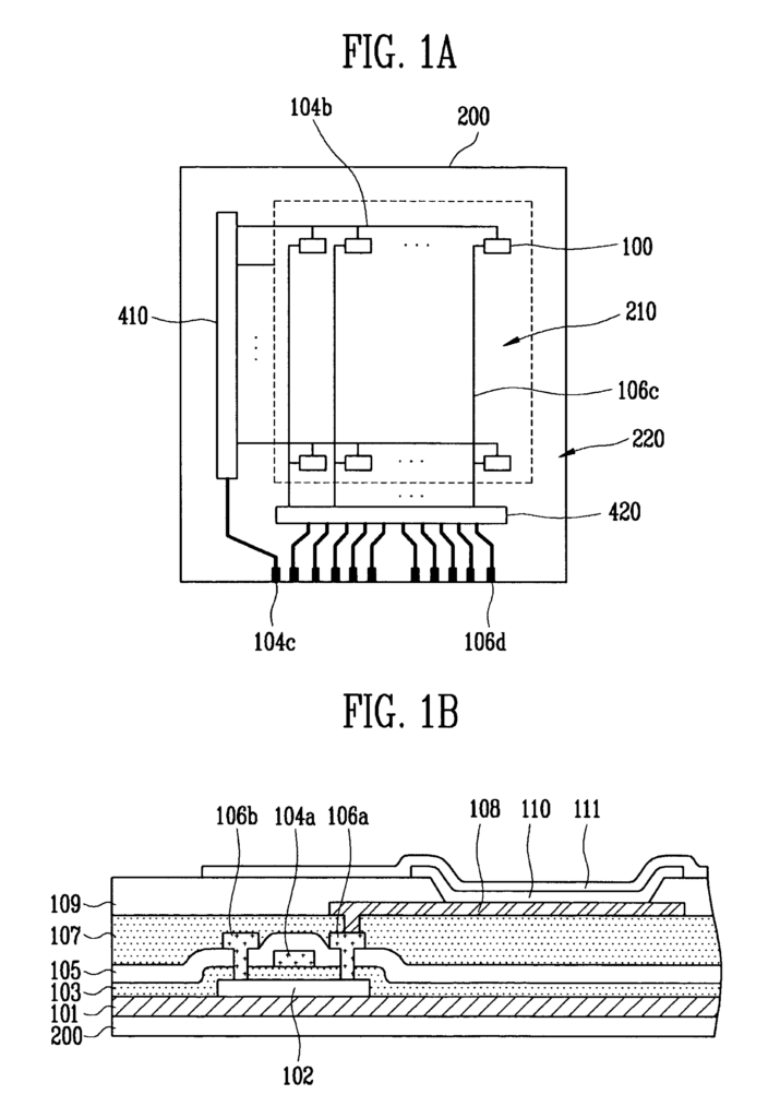
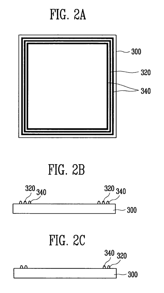
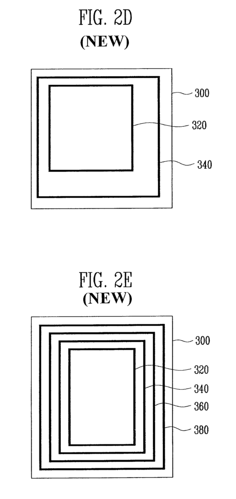
An aspect” of the invention is an organic light emitting display device. The device comprises a first surface, an array formed of organic light emitting pixels over the first surface, and a secondary substrate placed on top of the first, with the array interposed between them. The device also includes a frit-seal interposed between a first substrate, a second substrate, and an array. A second frit-seal interposed between a first substrate, a second substrate, and an array.
In the device described above, each of the two frit seals may form a loop closed around the array. The second frit sealing may surround the initial frit sealing. The device can also include a third seal that is interposed between the two substrates and configured to encircle the array. The third seal can be attached either with or with out a layer between the first and second substrates. The third fritseal may surround the two first fritseals. The device can also include a fourth seal that is interposed between the first and second substrates and configured to surround array. The combination of the first substrate, second substrate, second fritseal, and third fritseal may create an enclosed space that is hermetically sealed.
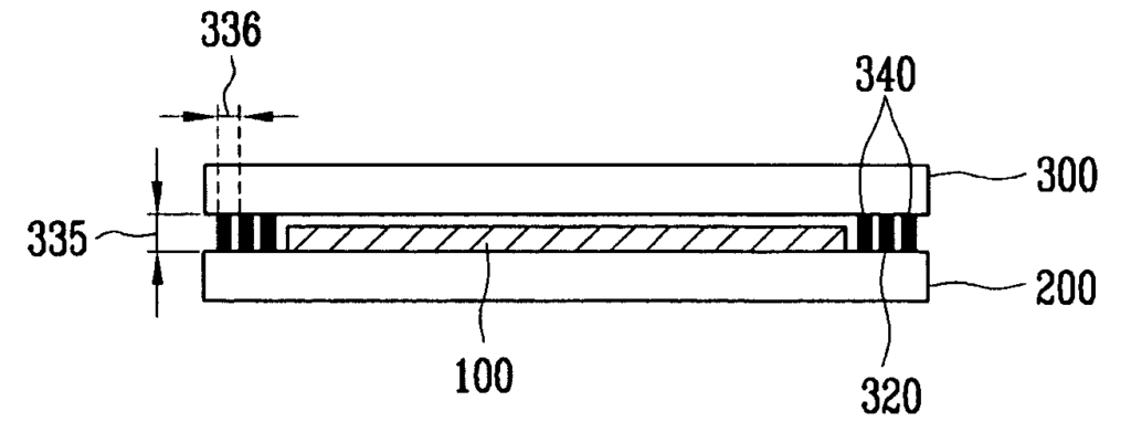
Still refering to the device described above. The device may consist of a segment where the first, third and second frit seals are substantially parallel. The height of the first fritseal may range from 10 m to 30 m. This height is measured perpendicularly to the surface of the first substrate that faces the second substrate. The first frit sealing may have a thickness of about 0.5 to 1.5 mm. This is measured parallel to the surface of the first substratum in the cross-sectional plane where the thickness is smallest. The first frit sealing may be separated from the second seal by a distance. However, the first seal can have a portion along which the distance remains constant. The distance along the portion where the distance is substantially constant can range from 10 m to 1000 m. The first frit can be separated from the second with a distance. This distance may vary along the first seal. Combining the first substrate, second substrate, first frit sealing and second frit sealing can define a substantially hermetic space. The enclosed space contains a gas that is not air. The device can also include a layer between the first frit and the first substrate. This layer may be made of an organic or inorganic substance.
Another aspect of the invention is a method for making an organic display device. This method involves providing an unfinished display device that includes a first surface and an array formed of organic light emitting pixel over the first surface, supplying a second base, and interposing this array between the two substrates. The method also includes interposing first frits between the two substrates, while enclosing the array. It then involves interposing second frits between the two substrates, while enclosing the array. Finally, it involves melting and solidifying a part of both the first frit and the second frit to connect the first substrate with the second substrate.
In the method described above, interposing of the array, interposing of the first frit, and interposing of the second frit can be performed essentially simultaneously. The first frit can be formed over either the first or the second substrate. The first frit can be interposed by forming it on the substrate first, with or with out a layer between the frit first and the substrate first. Similarly, the second Frit can be interposed by forming it on either the substrate first with or with out a layer between the frit second and substrate first. The method can also include interposing a second frit between the second and first substrates, while surrounding the first frit. The first, the second and the third frits can extend in a substantially parallel direction.
The method may still further include cutting the resulting product into two or multiple pieces, wherein one of the pieces comprises an array encapsulated between a cut piece of the first substrate and a cut piece of the second substrate and two or three frits. The method can still include cutting the product into two pieces. One of these pieces may contain an array enclosed between a first substrate cut, a second substrate cut, and two or three frits.
Hereafter, preferred embodiments of the present invention with reference to the accompanying drawings will be described. When one device is connected with another, it can be directly connected or indirectly connected via another device. For clarity, we have omitted irrelevant devices. Like reference numbers refer to similar devices throughout.
The organic light-emitting display (OLED), is a display consisting of an array organic light-emitting diodes. Organic light emitting devices are solid-state devices that include organic materials and are adapted for generating and emitting light when electrical potentials are applied.
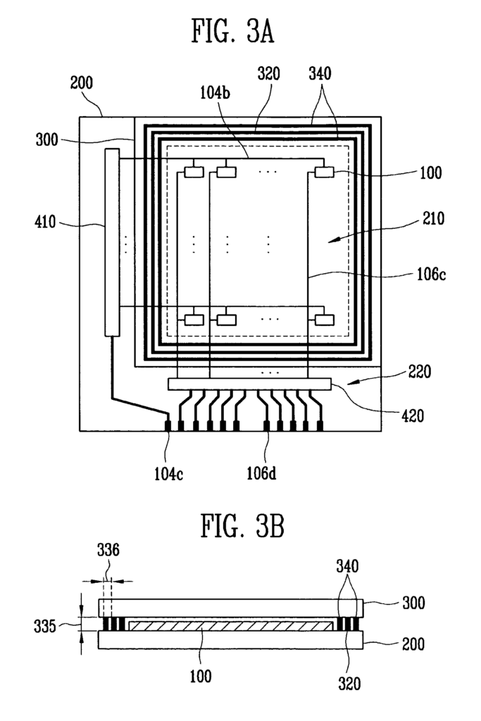
OLEDs are generally classified into two types based on how the electrical current stimulating the display is delivered. FIG. FIG. FIG. FIG.4B shows a simplified version of the active matrix type OLED 1001. Both configurations include OLED pixels overlaid on a substrate 1002. The OLED pixels have an anode, a cathode, and an organic layer. “When an appropriate electrical current (current) is applied to anode 1004, an electric current flows through pixels, and visible light is produced from the organic layer.
Referring to FIG. The passive matrix OLED design (PMOLED), shown in Figure 4A, includes elongate anode strips 1004 that are arranged perpendicularly to elongate cathode strips 1006, with organic layers between them. The intersections between the strips of cathode and anode define individual pixels of OLED, where light is produced and emitted when the strips of anode and cathode are appropriately excited. The PMOLEDs are relatively easy to manufacture.
Click here to view the patent on Google Patents.
Leave a Reply