Invented by Chih-Che Kuo, Wei-Sheng Hsu, Chun-Yen Hsiao, Teco Nanotech Co Ltd
Field-emission displays are a type of display technology that uses electron emission from a cathode to produce an image. This technology is commonly used in televisions, computer monitors, and other electronic devices. The carbon nanotube cathode is a key component of field-emission displays, as it provides the electrons necessary for the display to function.
The sintering method is becoming increasingly popular in the production of carbon nanotube cathodes for field-emission displays due to its many advantages. One of the main advantages of this method is that it produces a highly uniform and dense structure, which results in a more efficient electron emission. This, in turn, leads to a brighter and clearer display.
Another advantage of the sintering method is that it is highly scalable, which means that it can be used to produce large quantities of carbon nanotube cathodes at a relatively low cost. This is particularly important in the field of display technology, where high-volume production is essential to meet the growing demand for high-quality displays.
The market for sintering method to carbon nanotube cathode for field-emission display is expected to continue to grow in the coming years. This growth is being driven by the increasing demand for high-quality displays in various applications, including televisions, computer monitors, and mobile devices.
In addition, the development of new and innovative display technologies, such as flexible and transparent displays, is also expected to drive the demand for carbon nanotube cathodes. These new technologies require highly efficient and reliable cathodes, which can be produced using the sintering method.
Overall, the market for sintering method to carbon nanotube cathode for field-emission display is a rapidly growing and highly promising market. With its many advantages and increasing demand, this technology is poised to become a key player in the field of display technology in the coming years.

The Teco Nanotech Co Ltd invention works as follows
A vacuuming-sintering method is disclosed for the formation of a carbon nanotube from a field display. An anode is attached as a cathode to an anode. The assembly is placed on a heating element in a vacuum furnace, with the cathode next to the heating element. Each anode and cathode have at least one electrode connection to an external voltage source. The vacuum sintering furnace’s internal pressure is decreased, the heating element activated, and a voltage is applied across the cathode/anode. This creates an electric field between the cathode & the anode. After the electric field has been formed, the voltage is turned off and continued heating is allowed for a predetermined time. The heating is stopped and the anode and cathode are removed from the vacuum furnace. This ensures that the carbon nanotube forms parallel to the electric fields and perpendicularly to the cathode. Alternatively, one end of the nanotube is inclined towards anode for advantage electron generation.
Background for Sintering method to carbon nanotube cathode for field-emission display
The present invention is a sintering process for a carbon-nanotube of a field emission display. More specifically, it relates to a method that uses a locking member to lock the cathode and anode structures. During vacuum sintering, a specific electric field is applied. The cathode structure of the carbon nanotube is inclined towards the anode at a smaller angle. The carbon nanotube attaches one end to the cathode, and the other is perpendicular.
Thin-film lithography is used to fabricate the conventional cathode structure for field-emission displays, such as the Spindt-type metal spike configuration. This type of field-emission displays has a threshold electric field that can reach hundreds of Volts per millimeter. The driving device’s cost is therefore high.
The aspect ratio of carbon nanotube structures is very high. The carbon nanotube’s gauge is usually several to tens or more nanometers. It can also reach several microns in length. The carbon nanotube can also be thermally stabled and stretched, making it a good source of electron emission for field-emission displays. The carbon nanotuble can be grown directly on the cathode electro by CVD. This method is already widely used. This technique employs catalytic metal to vertically deposit carbon nanotubes on the cathode electro. Then, a patterning process is used to create uniform carbon nanotubes. This allows for a current density of tens of to hundreds of milliamps per square cm. This technique has a limit due to the structure and material factors. However, it can produce a threshold electric field of 10V/?m. This technique is currently only possible on silicon wafers and is not widely commercialized.
Another common nano-technology is arc discharge. An arc discharge can create a carbon nanotube that is more suitable for field emission displays. Combining screen printing with coating reduces threshold voltage to below 2V/m. To form the electron emission source, the carbon nanotube is patterned on the cathode electrode’s surface. The thick carbon nanotube film formed by coating technique causes terminal disorder. The electron emission density is not uniform. Therefore, electrons generated at higher terminals can easily create shielding effects on neighboring terminals. This affects electron generation at the nearby terminals. The adhesion material used to attach the carbon-nanotube to the cathode electro can also affect the distribution and dispersion of the carbon nanotube.
A vacuum sintering technique is currently available that allows the carbon nanotube to be attached directly to the cathode electro. This eliminates the problems caused by adhesion materials and coatings. To increase electron density, you can increase the density the carbon nanotube. Interleaving and interference can occur between the carbon nanotubes when they are randomly applied to the cathode substrate. The application of an electric field cannot attach one end of the carbon-nanotube vertically to the substrate.
A vacuuming sintering technique is used to form a carbon nanotube for a field display. An anode is attached as a cathode to an anode. The assembly is placed on a heating element in a vacuum furnace, with the cathode next to the heating element. Each anode and cathode have at least one electrode connection to an external voltage source. The vacuum sintering furnace’s internal pressure is decreased, the heating element activated, and a voltage is applied across the cathode/anode. This creates an electric field between the anode and cathode. After the electric field has been formed, the voltage is turned off and continued heating is allowed for a predetermined time. The heating is stopped and the anode and cathode are removed from the vacuum furnace. This ensures that the carbon nanotube forms parallel to the electric fields and perpendicularly to the cathode. Alternatively, one end of the nanotube is inclined towards anode for advantage electron generation.
The heating element may include an infrared ceramic heating panel, for example. A vacuuming step may be performed to bring the vacuum sintering oven to 10?5 torr. A cathode is a first conductive layer that has been formed on a substrate. This serves as the cathode electrode. Material whose melting point has been lowered in vacuum to enable the carbon nanotube embedded within it is cathode material. This material can include copper, aluminum and silver as well as gold and chromium. An electrode lead connects the first conductive layer with a voltage source. A step is taken to coat a carbon nanotube on top of the first conductive layers on the first conductor layer. The cathode is made up of a glass substrate and a silicon wafer. An electrode lead is connected to the voltage source in the glass substrate of a cathode. Anode comprises a first conductive coating on a substrate. The first conductive coat can be ITO, chromium, or aluminum. To maintain a predetermined distance between the anode an the cathode, the method also includes forming a spacer.
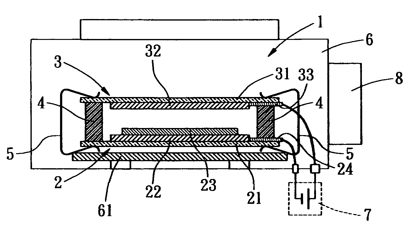
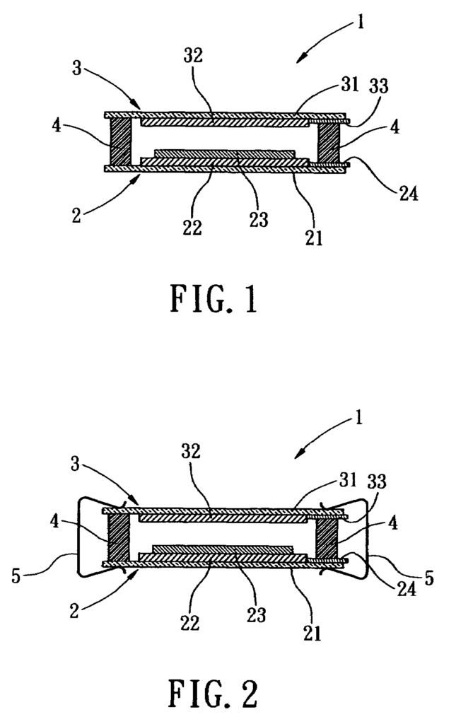
FIGS. “FIGS. Directly sintered carbon nanotubes are used in the field-emission display. The electron emission sources of carbon nanotubes formed on the cathode structures 2 and 1 of the field-emission display are randomly applied to the cathode structures 21 and 2. Interference and interleaving effects result, so that the one end of each carbon nanotube cannot properly be perpendicularly attached by the electric field.
In this embodiment, the first conductive layer 22 of the cathode structures’ glass substrate 21 is formed. The cathode electrode’s melting point can be decreased in vacuum to form the first conductive layer 22, which allows the carbon nanotube to be embedded. For example, the material for the cathode electrode can be copper, silver, gold, or chromium. An electrode line 24 is located on the opposite side of the first conductive layers 22 and 21. It transmits a control voltage to the 22nd conductive layers 22.
A carbon nanotube layer is applied to the first conductive layer 22, A carbon nanotube solution can also be prepared to form the second layer of the electron emission source.
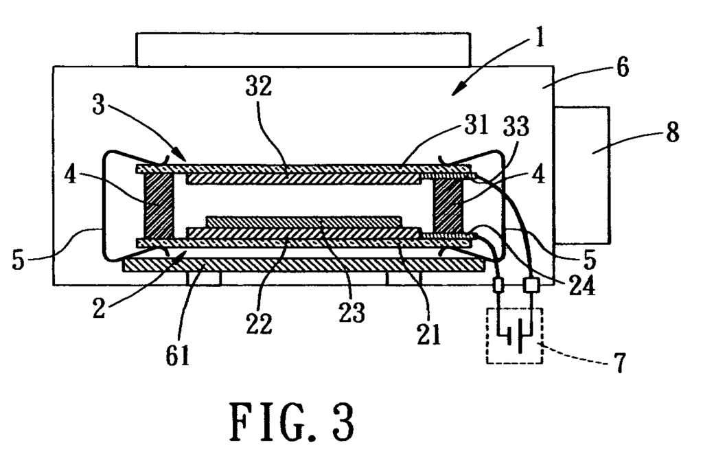
An anode 3 is placed to face the electron emission source and align with it. For example, the substrate 31 of anode 3 is made from heat-resistant silicon wafer or glass. To form an electric field, a first conductive layer 32 must be formed on substrate 31. Conductive material, such as ITO or chromium. An electrode line 33 is located on the opposite side of the conductive layer to the glass substrate 31 and transmits control voltage to the first layer 32.
A spacer is created between the anode 3, and the cathode structures 2, to maintain a constant distance between them. This allows for a uniform electric field to be formed by the voltage between the cathode 2 & the anode 3.
A fastening member 5, is available for attaching cathode 2 to the anode 3.
FIG. 3. This is the vacuum sintering of the cathode. The assembled anode and cathode are placed on the heating element (infrared clay) 61 of vacuum sinter furnace 6. The glass substrate 21 is located adjacent to the heating element 61.1, and the electrode wires 33 and 24 are connected to the external voltage source 7 via a heat-resistant conductor wire.
Click here to view the patent on Google Patents.
Leave a Reply