
Invented by Dong Woo Kim, Yong Chun Kim, Hyun Kyung KIM, Samsung Electronics Co Ltd
Vertical Type Nitride Semiconductor LEDs are designed with a vertical structure, where the light emission occurs perpendicular to the substrate. This design allows for better heat dissipation, resulting in improved efficiency and longer lifespan compared to traditional lateral-type LEDs. The vertical structure also enables better light extraction, leading to higher brightness and enhanced color rendering capabilities.
One of the key factors driving the market for Vertical Type Nitride Semiconductor LEDs is the increasing demand for energy-efficient lighting solutions. LED lighting has gained popularity as a sustainable alternative to traditional incandescent and fluorescent lights. The superior energy efficiency of Vertical Type Nitride Semiconductor LEDs makes them an ideal choice for residential, commercial, and industrial lighting applications, as they consume significantly less power while providing high-quality illumination.
Another significant factor contributing to the market growth is the rising demand for displays and signage. Vertical Type Nitride Semiconductor LEDs offer excellent color uniformity, high contrast ratio, and wide viewing angles, making them suitable for various display applications. From large outdoor billboards to small indoor screens, these LEDs provide vibrant and eye-catching visuals, enhancing the overall viewing experience.
The automotive industry is also a major driver of the Vertical Type Nitride Semiconductor LED market. With the increasing adoption of electric vehicles (EVs) and the growing focus on energy-efficient lighting in automobiles, the demand for high-performance LEDs is on the rise. Vertical Type Nitride Semiconductor LEDs offer superior brightness, longer lifespan, and better thermal management, making them ideal for automotive lighting applications such as headlights, taillights, and interior lighting.
Furthermore, the market for Vertical Type Nitride Semiconductor LEDs is expected to benefit from the ongoing advancements in technology. Manufacturers are continuously investing in research and development to improve the efficiency, color accuracy, and overall performance of these LEDs. This includes innovations in chip design, packaging techniques, and phosphor materials, among others. As a result, Vertical Type Nitride Semiconductor LEDs are becoming more affordable and accessible, further driving their market growth.
In conclusion, the market for Vertical Type Nitride Semiconductor LEDs is witnessing significant growth due to their superior energy efficiency, long lifespan, and high brightness. The increasing demand for energy-efficient lighting solutions, displays, signage, and automotive lighting is driving the adoption of these LEDs. With ongoing technological advancements and cost reductions, the market is expected to continue expanding in the coming years.
The Samsung Electronics Co Ltd invention works as follows
The present invention discloses a vertical nitride type semiconductor light emitting device. The nitride light emitting diode includes an n type nitride layer, an active nitride layer under the n type nitride layer, a sub-layer of p-type semiconductors formed below the active layer and an n side electrode comprising a bonding pads formed adjacent to the edge of the upper surface of n type nitride layer and atleast one extended electrode in a band formed from the bonding pads. The bonding pad is adjacent to the upper edge of the nitride layer, which acts as a light-emitting surface. This prevents a wire from blocking light from the active layer. The extended electrode is available in various shapes and can prevent current concentration.
Background for Vertical Type Nitride Semiconductor Light-Emitting Diode
1. “1.
The present invention is a vertical nitride type semiconductor light-emitting diode. More specifically, it is a vertical nitride type semiconductor light-emitting diode that has a bonding plate of an electrode on the n side formed adjacent to the edge of an upper surface n type nitride layer, serving as the light-emitting surface. This prevents a wire-bonding portion from blocking light from the light-emitting surface. It also has an extended electrode n side electrode nside extended in different shapes, and n n n n n n n n n n n n n n n a n n n n n n n n n nside electrode n n n n n nside electrode nside electrode nside electrode nside electrode nside electrode nside electrode nside electrode extended electrodes n-side bonding pads
2. “2.
The term nitride refers to any III-V group crystal semiconductor, including GaN, InN and AlN. It is used for light emitting devices that emit light within a narrow wavelength range, from ultraviolet to green, but especially blue.
The nitride light-emitting diode can be manufactured using an insulating substrate such as sapphire, which meets the requirements of lattice matching for crystal growth. It has a horizontally aligned structure, in which the two electrodes connected to the p-type and the n-type semiconductor layers are arranged substantially horizontally to the upper surface of a light-emitting structure.
The horizontal structure of the nitride light emitting diode is a disadvantage. The first is that a narrow path of electric current in the horizontal direction, from an n side electrode to a P side electrode through an “active layer”, is formed. The nitride light-emitting diode with the horizontal structure has a higher forward voltage (Vf) due to the narrow path for electric current.
The diode is unstable because of mechanical stress between the sapphire and nitride light emitting structures. This is due to the increased heat generation caused by the increase in current density.
The nitride-semiconductor light-emitting diode with the horizontal structure is characterized by a smaller light-emitting area. This reduces the light-emitting efficiency, depending on the brightness of the diode.
In order to increase the disadvantages of nitride light-emitting diodes with horizontal structures, a vertical nitride light-emitting diode has been developed from which the sapphire is removed using a laser lift off process.
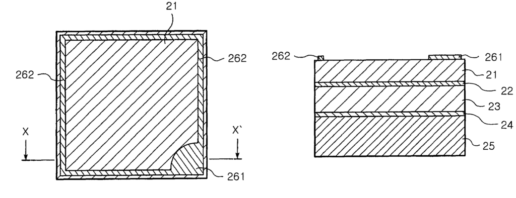
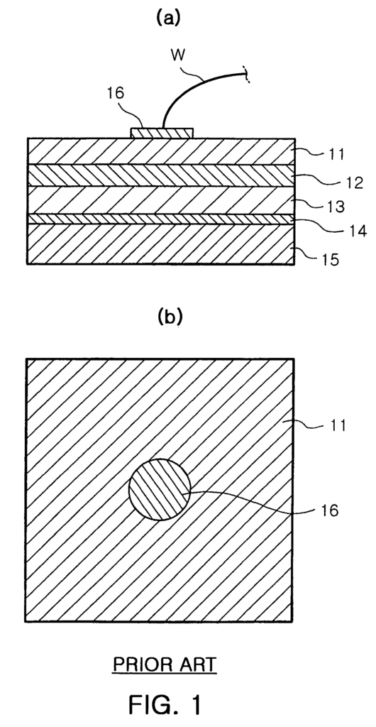
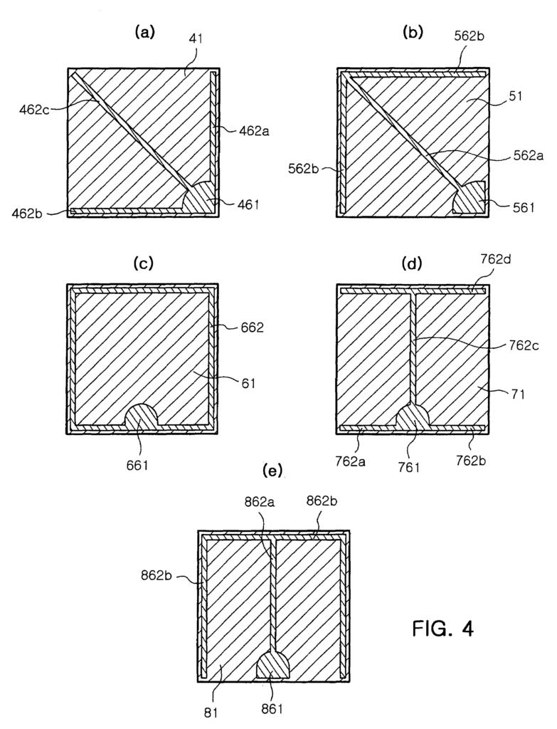
FIGS. The top and side views of FIGS. 1 a and b illustrate a vertical type conventional nitride light emitting semiconductor. Referring to FIGS. In order to manufacture the conventional nitride light-emitting diode using a n-type layer, an active layer, a p type nitride, and an n-type layer, FIGS. The n-type layer 11 is the uppermost layer in this construction. Its upper surface serves as the light emitting surface. The conventional nitride light emitting device comprises the nitride layers 11, 12, 13, and 14, a conductive layer 14 and a conductive substrate 15, sequentially arranged from the top. The nitride light emitting diode 13, in addition, comprises an n side electrode 16 that is formed on the upper surface of n type nitride layer 13 so as to provide a wire bonding section for supplying an electric current.
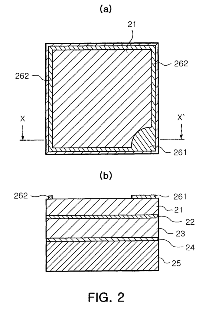
As shown in FIGS. As shown in FIGS. “When the n side electrode 16 is formed in the middle of the upper surface n type nitride layer 11, a problem occurs because a wire W attached to the n side electrode 16 via wire bonding blocks light from the upper surface n type nitride layer 11.
The excellent conductivity in the nitride layer 11 causes the current density to be concentrated at the bottom of n side electrode 16, thereby reducing the effective area of light emission.
The n-side of the electrode is formed next to the edge of the n type nitride layer, while maintaining an effective distribution of current.
The present invention was made to address the problems mentioned above. Its object is to create a flip-chip light-emitting diode with a new electrode design that places an n side electrode adjacent to the edge of an N-type nitride layer, while maintaining an effective distribution of current. This will increase the efficiency of light-emitting.
According to one aspect of this invention, these and other objectives can be achieved by providing a vertical nitride type semiconductor light-emitting diode that comprises: an ntype nitride layer; an active ntype nitride layer formed beneath the ntype nitride layer; a Ptype nride layer formed underneath the active layer; and a nside electrode consisting of a bonding pads formed adjacent to the upper surface edge
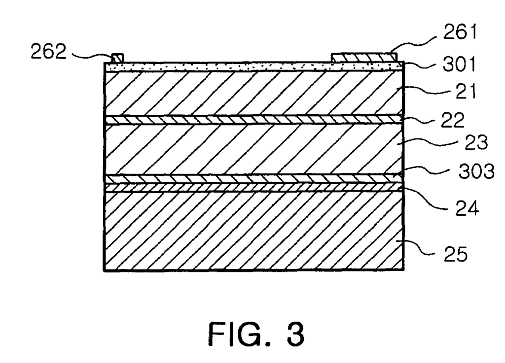
The nitride-semiconductor light emitting device may also include a buffer between the n type nitride layer and the n side electrode. The nitride light emitting diode can further include a transparent electrode formed between the n type nitride layer and the electrode n. The transparent electrode may be made of a material that allows for effective current spread while still allowing for light transmission. The transparent electrode layer can be composed of at least one oxide layer selected from the group consisting indium tin oxide (ITO), zinc based oxide ZnO, tin oxide SnO2, and indium zinc based oxide IZO.
The nitride light emitting device may also include a conductive substrate under the p type nitride layer. The nitride light emitting diode can now include a conductive layer between the conductive substrate and the semiconductor layer.
The nitride-semiconductor light emitting device may also include a highly reflective, ohmic layer disposed under the p type nitride layer. The highly reflective ohmic layer can be made of a material that reflects light from the active layer to the n-type semiconductor layer, which is used as the light emitting layer. This will increase brightness and provide an ohmic connection with the p type nitride layer. The material can be Ag, Ni Al, Rh Pd Ir Ru Mg Zn Pt Au or combinations thereof.
In general, the nitride light emitting diode is rectangular in cross-section. The upper surface is rectangular because the uppermost layer is the n type nitride layer. The vertical type nitride-semiconductor light-emitting diode of the present invention may be constructed in different ways.
As an example, “the n side electrode” may include a bonding plate formed adjacent to a corner of upper surface of n type nitride layer and a first electrode formed along four sides of upper surface of n type nitride layer. The n side electrode can also include a plurality second extended electrodes, which are formed by a portion from the first electrode that is formed on one side along the upper side of n type nitride layer and another portion formed along the opposite side.
As another example of an n side electrode, it may consist of a bonding plate formed adjacent to a corner of upper surface of n type nitride layer. First and second extended electrodes are formed along the upper surface where the bonding plate is formed.
Click here to view the patent on Google Patents.
Leave a Reply