Invented by Kwan-Hee Lee, Samsung Display Co Ltd
The Samsung Display Co Ltd invention works as follows
The present invention relates a two-sided light emitting organic EL device that includes a reflection sheet with an opening, and a first electrolyte formed in the opening. On the first electrode there is an organic layer, and on top of the organic layer a second electrode. The opening corresponds with a central part of the first electrode.

Background for Double-sided organic electroluminescence device with a reflective layer and fabrication methods thereof
1. “1.
The present invention is a two-side organic electroluminescence device that emits light from both sides. More specifically, it is a two-side organic electroluminescence device with a reflection layer arranged beneath a first electrode.
2. “2.
In general, an organic electroluminescence display device (EL) is a flat panel display that emits light when an organic compound is electrically excited. It can be fabricated with a low temperature. It has a fast response time of less than 1 ms, low power consumption and a large viewing angle because it is self-emitting. It can be made thin and light, since it does not require a backlight like a LCD. It can be used for products like cellular phones. It is a good choice for cellular phones and other products due to its uniform surface lighting characteristics.
The organic light-emitting layers are sandwiched between the anode (the anode) and cathode (the cathode). The organic light emitting layer combines holes from the cathode with electrons in order to form excitons. These are hole-electron pair.
Generally, an Organic EL Display Device may be a Passive Matrix or Active Matrix device depending on the method of driving N XM pixels arranged in a matrice. The passive matrix organic EL displays are used for low-resolution displays, since the display region is built in a simple matrix using anodes and cascades. Active matrix organic EL displays include at least two thin-film transistors for each pixel. The active matrix display can exhibit a more stable luminance because it supplies a constant current regardless of the number pixels. It is also used for large displays with high resolution due to its low energy consumption.
The organic EL displays can be classified as bottom-emitting or top-emitting devices based on the direction in which light is emitted by an organic light emitting layer. The bottom light emitting device emits the light towards the substrate. A reflection electrode is formed in the upper part of an organic light-emitting film, while a transparent electrode forms the lower part. The light emitting surface of an active matrix organic light emitting device can be reduced because the thin-film transistors in each pixel are not light emitting. The luminance of a top-light-emitting organic EL device can be improved by increasing the light transmission area. This is done by forming a reflective electrode on a lower portion of an organic-light-emitting-layer and a transparent electrode in the upper part. Currently, a two-side organic EL display that can simultaneously realize top light emission and lower light emission on a single substrate is being recognized as a new generation flat panel display.
FIG. “FIG.
Referring to FIG. The conventional two-side organic EL display device comprises a first transparent layer 110, and a pixel defining film 130 that is formed on top of the first electrode to expose the electrode. “Light can be emitted from the front and back sides of the display device where the first transparent electrode 110 is formed. This is done by sequentially forming a film layer that includes an organic light emitting layer and a second electrode on the first transparent electrode 110.
The “both-side organic EL display” and a method of fabrication thereof will be described below in detail with reference to FIG. The two-side light emitting organic EL display device and a fabrication method thereof are described in detail below with reference to FIG. 3.
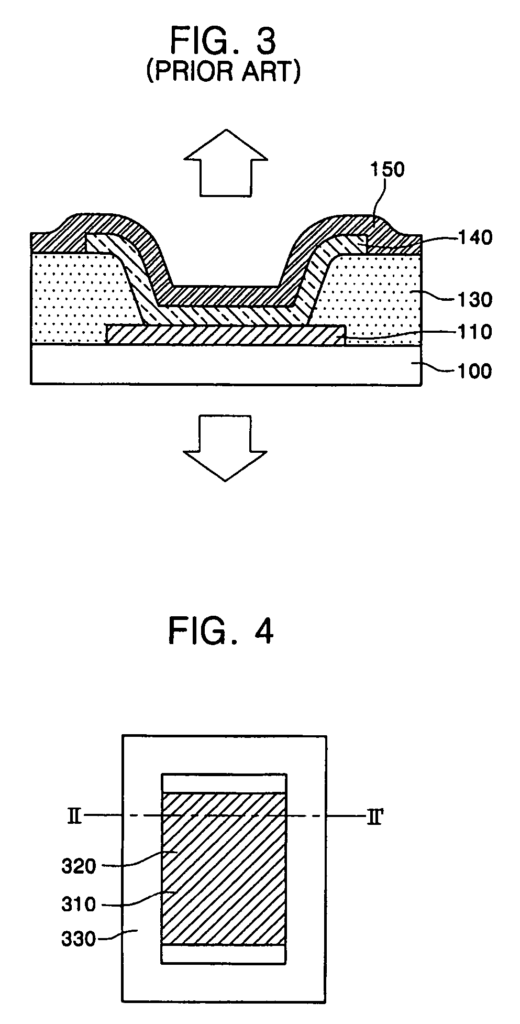

FIG. FIG. Figure 1 shows a conventional both-side light emitting organic EL display device. FIG. “Figure 3 shows a cross-sectional view of a conventional two-side organic EL device, and a fabrication method.
Referring to FIG. The first electrode 110 of FIG. 2 is patterned onto a substrate made from glass or plastic. When the first electrode is an anode, it is a transparent electrolyte that can be made of indium tin or indium zinc oxides (IZO) which have high work functions. “When the first electrode is a cathode it can be formed as a transmitting electrode made of a material selected among Mg, Ca Al and Ag alloys as a conductive metallic having a low-work function.
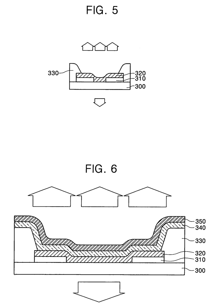
On the first electrode 110, a pixel-defining layer 130 can be formed to partially expose the surface of first electrode.
FIG. “FIG. “2 in which a second electrode is formed on top of the first electrode exposed and the pixel-defining layer.
Referring to FIG. On the first electrode 10 exposed, an organic film 140 containing at least an organic layer emitting light is formed. The organic film layer may also include a hole injecting layer, a transporting layer for electrons, and an electron injection or transporting layer.
The second electrode 150 will be formed over the entire organic film layer. When the first electrode 10 has a transparent cathode, the second electrode may be a transmission electrolyte made of a conductive material with a low-work function, such as Mg, Al, or Ag.
A conventional two-side organic EL display may emit light from only a portion where the first electrode has been formed. A small amount of light generated may be emitted and the life of the device could be reduced as a result, since the area where the first electrode has been formed can be small.
The present invention is a two-sided light emitting organic EL device that increases the light emitted through the formation of a portion on a reflective film of a first electrolyte.
Additional features will be described in the following description and will in part be evident from the description or can be learned through the practice of the invention.
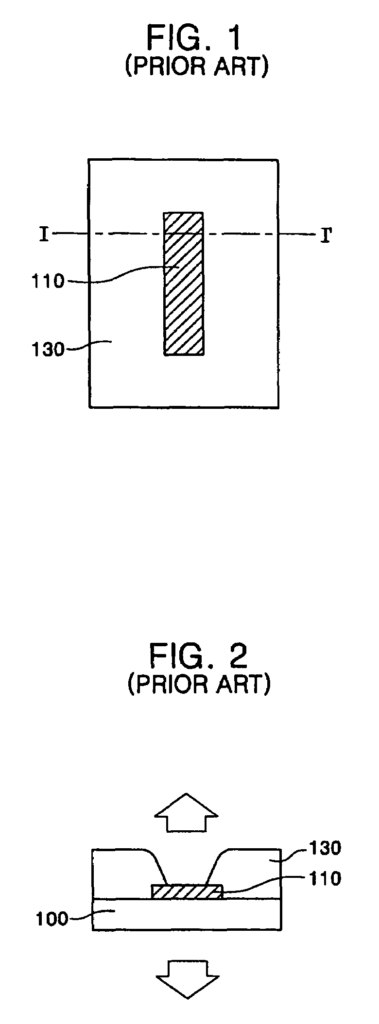
The present invention discloses a organic EL display including a substrate; a reflection sheet arranged over the substrate with an opening therein, a first electrolyte arranged in the opening and on the reflection sheet, the opening corresponding a central part of the electrode; a pixel defining film for exposing a portion of the electrode; an organic layer arranged above the organic layer comprising an organic light emitting layer.

The present invention also provides a fabrication method for an organic EL device, including forming a reflective layer with an opening; forming a 1st electrode in the opening which corresponds to the central portion of the 1st electrode; forming a pixel defining layers on the 1st electrode to expose a small part of it, forming a organic layer which includes at the very least an organic light emitting layer on that exposed part, and forming a 2nd electrode on that organic layer.