Invented by Prasoonkumar Surti, Karthik Vaidyanathan, Atsuo Kuwahara, Hugues Labbe, Sameer KP, Jonathan Kennedy, Joydeep Ray, Travis T. Schluessler, John H. Feit, Nikos Kaburlasos, Jacek Kwiatkowski, Tomer Bar-On, Carsten Benthin, Adam T. Lake, Vasanth Ranganathan, Abhishek R. Appu, Intel Corp
The Intel Corp invention works as follows
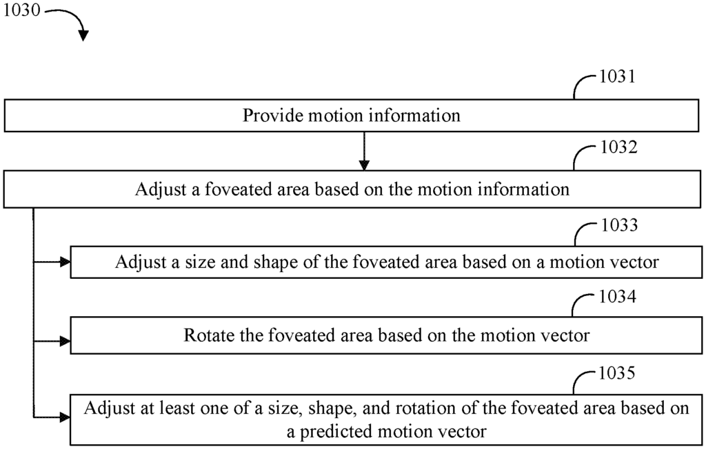
Systems, devices and methods” may include technology that assigns the first shading rate to the first region of an image frame. This technology also assigns a secondary shading rate to the second region of a frame. The first shading rates indicates that the region in question will be rendered with a certain resolution. And the second shading rates indicates that a lower resolution will be used for the second region. The first and the second shading rates are linked to a selection that is based on an object’s motion vector. The object is rendered in a scene which includes the first area rendered at first resolution and second region rendered with second resolution.

Background for Motion biased Foveated Renderer
Current parallel graphic data processing includes methods and systems developed to perform specific operations such as linear interpolation. tessellation. rasterization. texture mapping. depth testing. Graphics processors traditionally used fixed-function computational units to process graphics. However, in recent years, some portions of graphics processing processors have become programmable. This allows them to support a greater variety of operations when processing vertex or fragment data.
Fovea” may refer to a depression on the retina where the visual acuity is highest. This region may have a high concentration of retinal cones, and thus the center of your field of vision. A fovea, or foveated region, may be a focus area in some graphics applications.
In the following description numerous specific details will be provided to give a better understanding of the invention. One skilled in the art will understand that the invention can be implemented without any of these details. Other times, well-known features are not described to avoid confusing the present invention.
System Overview
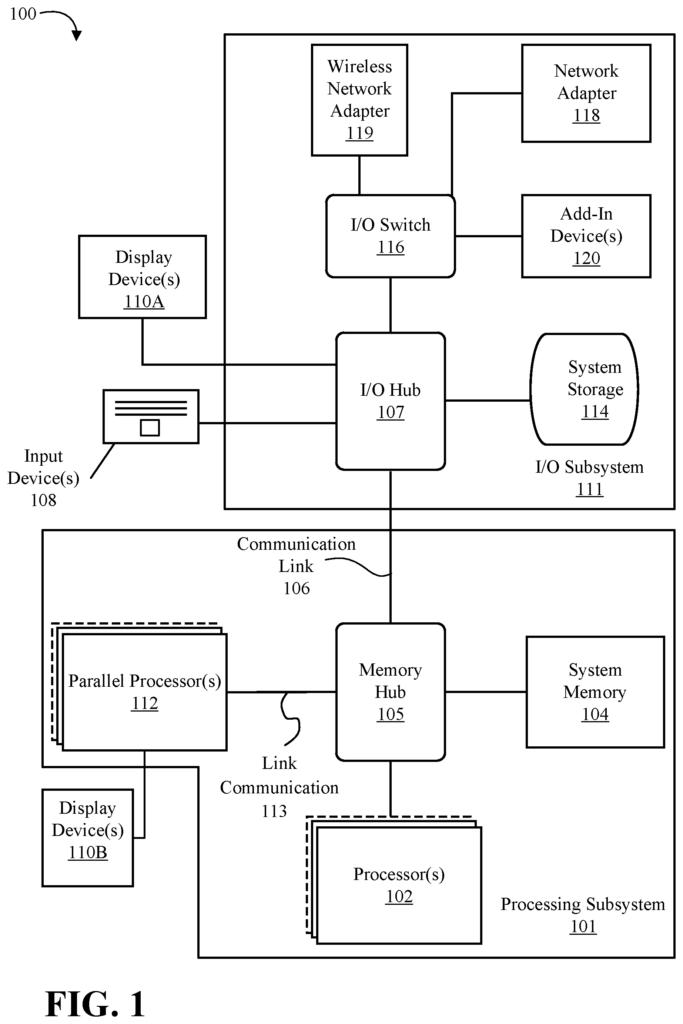
FIG. “FIG. A processing subsystem 101 is included in the computing system 100. It includes one or more processors 102 and a system storage 104. They communicate via an interconnection path, which may include a memory hub (105). The memory hub 105 can be either a separate component of a chipset or integrated into the processor(s) 102. Through a communication link 106, the memory hub 105 can be connected to an I/O system 111. I/O subsystem 111 also includes an I/O hub 107 which can allow the computing system 100 receive input from one or multiple input devices (108). The I/O hub (107) can also enable a display controller to be connected to the processor(s). 102 to provide outputs to the display device(s). 110A. One embodiment of the I/O hub107 and one or more display devices 110A can be combined with an embedded, local, or internal display device.
In one embodiment, the processing subsystem 100 includes one or multiple parallel processors 112 coupled with memory hub 105 by a bus or another communication link 113. Communication link 113 can be any of a number of standard-based communication technologies or protocols such as PCI Express or vendor-specific communications interfaces or communications fabrics. In one embodiment, the one or multiple parallel processors 112 form a computingly focused parallel or a vector processing system. This may include a large amount of processing cores or clusters such as a multi-integrated core (MIC). In one embodiment, the one-or-more parallel processor(s 112) form a graphics subsystem which can output pixels via the I/O hub 107 to the one (or more) display device(s 110A. The one or multiple parallel processors 112 may also include a display interface and controller (not shown), allowing a direct connection with one or several display devices 110B.
In the I/O subsystem 112, a system storage device 114 can be connected to the I/O hub107 to provide a storage system for computing system 100. An I/O switch (116) can be used as an interface mechanism to allow connections between I/O hub107 and other components. This includes a network adapter/wireless network adapter (118/119), which may be integrated into platform, and many other devices that can added via add-in devices 120. The network adapter (118) can be either an Ethernet adapter, or another wired networking adapter. Wireless network adapter 119 may include one or several of Wi-Fi, Bluetooth or near field communication (NFC) devices or any other network device that includes one, or more, wireless radios.
The computing system 100 may include additional components that are not shown. These could include USB or other ports connections, optical storage drives and video capture devices. The communication paths connecting the components of FIG. 1. may be implemented using any of the suitable protocols, including PCI (Peripheral Complement Interconnect) based protocols (e.g. PCI-Express) or any other bus/point-to-point communication interfaces or protocols(s), like the NV Link high-speed interconnect or interconnect protocols that are known in the art.
In one embodiment, one or more parallel processing units 112 include circuitry that is optimized for graphics and videos processing, such as video output circuitry. This constitutes a graphics processor unit (GPU). In a second embodiment, the parallel processors 112 include circuitry that is optimized for general-purpose processing while maintaining the computational architecture described herein. In a further embodiment, the components of computing system 100 can be integrated on an integrated circuit with other system elements. The one or more parallel processing units, 112 memory hub 105 and processor(s) 102 can all be integrated in a single integrated circuit. The components of the computing systems 100 can also be integrated in a single package, forming a “system-in-package” (SIP) configuration. In one embodiment, at least a part of the components of computing system 100 may be integrated into a Multi-chip Module (MCM), and this MCM can then be connected to other MCMs into a modular computer system.
It will be understood that the computing system 100 illustrated herein is only an illustration and that modifications and variations are possible. You can modify the connection topology including the number and arrangement for bridges, processor(s), 102, and parallel processor(s), 112, as needed. In some cases, system memory (104) is directly connected to processor(s), 102 via a bridge. Other devices, however, communicate with system memory (104) via the memory hub and processor(s), 102. Other topologies allow the parallel processor(s), 112, to be connected to either the I/O hub107 or directly one or more of the processor(s), 102 rather than the memory hub105. Other embodiments may include the I/O hub (107) and memory hub (105), which can be combined into one chip. One embodiment may have two or more processor(s), 102 connected via multiple sockets. These processors can be paired with one or more instances the parallel processor(s), 112.

Some components listed herein may not be available in all versions of the computing system 100. You may support as many add-in cards and peripherals as you like, or eliminate certain components. Other architectures might use different terminology for components than those shown in FIG. 1. In some architectures, the memory hub (105) may be called a Northbridge, while the I/O center 107 may be called a Southbridge.
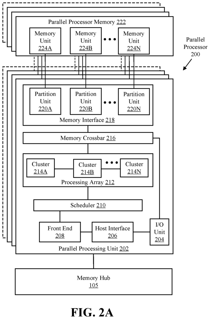
FIG. 2A shows a parallel processor 200 according to an embodiment. One or more integrated circuit devices may be used to implement the various components of the parallel process 200, including programmable processors, field-programmable gate arrays or application-specific integrated circuits (ASICs). The parallel processor 200 illustrated in FIG. 1. According to an embodiment
In one embodiment, the parallel processor 200 includes an I/O unit 204 that allows communication with other devices including other instances of the parallel processing unit. A parallel processing unit also includes an I/O 204 which allows communication with other devices, such as other instances of parallel processing unit 200. The I/O device 204 can be connected directly to other devices. One embodiment of the I/O device 204 connects to other devices using a switch or hub interface, such memory hub 105. The communication link 113 is formed by the connections between the I/O units 204 and the memory hub 105. The parallel processing unit 200’s I/O unit204 connects to a host interface (206) and a memory crossbar (216). Here, commands are received from the host interface to perform processing operations, while commands to the memory crossbar 226 are directed at performing memory operations.
When the host 206 receives commands via an I/O unit, it can direct the front end 208 to execute those commands. In one embodiment, the front end 208 is coupled with a scheduling 210 that distributes commands or other items of work to a processing array 212. In one embodiment, the scheduler ensures that the cluster array is configured correctly and in a valid condition before tasks are distributed. In one embodiment, the scheduler is implemented by firmware logic running on a microcontroller. The scheduler 210 implemented on a microcontroller is configured to perform complex work distribution and scheduling operations at fine and coarse granularity. This allows for rapid context switching and preemption of threads running on the processing array. In one embodiment, a host software can schedule workloads on the processing array using one or more graphics processing doorbells. The scheduler logic in the scheduler microcontroller can automatically distribute the workloads across the processing array.
The processing cluster array 212 can contain up to?N” Processing clusters (e.g. cluster 214A and cluster 214B through cluster 214N). The clusters 214A-214N can run a large number concurrent threads. The scheduler 220 can assign work to clusters 214A-214N from the processing cluster array 212, using different scheduling and/or work allocation algorithms. These may vary depending upon the type of program or computation being executed. The scheduler 210 can manage the scheduling dynamically or in part with compiler logic when compiling program logic for execution by processing cluster array 212. One embodiment allows for different types or types of programs to be processed by different clusters 214A-214N.
The processing cluster array 212 can be configured to perform different types of parallel processing operations. One embodiment of the processing cluster array is designed to perform general-purpose parallel computation operations. The processing cluster array 212 may include logic that can be used to perform processing tasks such as filtering video and/or audio, modeling operations including physics operations and data transformations.
In one embodiment, the processing cluster array212 is designed to perform parallel graphics processing operations. The processing cluster array 212 may include additional logic that supports the execution of graphics processing operations in embodiments where the parallel processor 200 can be configured to execute them. This includes texture sampling logic to perform texture operations as well as tessellation and other vertex processing logic. The processing cluster array 212 can also be used to run graphics processing-related shader programs, such as vertex shaders and tessellation shadesrs, geometry shadingrs, and pixelshaders. Parallel processing unit 202 can transfer data to system memory via I/O unit. 204 is used for processing. The transferred data can be saved to on-chip memory during processing (e.g. parallel processor memory 222) and then written back into system memory.
In one embodiment, the parallel processing unit (202) can be used to process graphics processing. The scheduler 210 can be set up to split the processing workload into roughly equal-sized tasks to make it easier to distribute the operations to multiple clusters 214A to 214N of the processing cluster array 212. Some embodiments allow for different processing to be performed on portions of the processing cluster array 212. One portion of the processing cluster array 212 may be used to perform topology generation and vertex shading. A second portion might be used to perform geometry shading and tessellation. The third portion could be used to shade pixels or perform other screen space operations to create a rendered image. Buffers may be used to store intermediate data from one or more clusters 214A to 214N, which can be transmitted between the clusters 214A to 214N for further processing.
The processing cluster array 212 may receive processing tasks during operation. This is done via the scheduler210. The scheduler receives commands from the front end 208 defining processing tasks. Processing tasks are data that describe how data will be processed. These include data indices, such as surface (patch), primitive, vertex, and/or pixels data. Also, state parameters and commands can be used to define the process (e.g. what program is to run). The scheduler 210 can be set up to retrieve the indices for the tasks, or it may get them from the front-end 208. Front end 208 can also be configured to ensure that the processing cluster array (212) is in a valid state prior to the workload specified by incoming commands buffers (e.g. batch buffers, push buffers etc.).
Each one or more instances the parallel processing unit 200 can be paired with parallel processor memory 222. The memory crossbar 226 can access the parallel processor memory 222. It can also receive memory requests from both the processing cluster array 212, and the I/O device 204. A memory interface 218 allows the memory crossbar to access parallel processor memory 221. Multiple partition units can be included in the memory interface 218 (e.g. partition unit 220A and partition unit 220-B) which can each couple to a specific portion of parallel processor memory 221 (e.g. memory unit 220-N). One implementation has the number 220A-220N partition units equal to the number memory units. For example, a first partition 220A has a corresponding 1 memory unit 224, a second 220B has the corresponding 284B memory unit, and an Nth 220N has the corresponding 284N memory unit 224. Other embodiments may have the number 220A-220N not equal to the number memory devices.
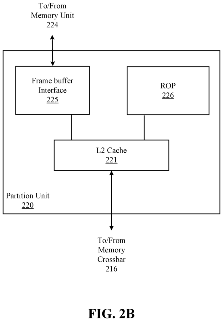

In different embodiments, the memory unit 224A-224N may include various memory devices such as dynamic random access memory or graphics random memory (DRAM), or synchronous graphics random address memory (SGRAM), and graphics double data rate memory (GDDR). The memory units 224A-249N can also contain 3D stacked memory. This includes but is not limited to high-bandwidth memory (HBM). The specific implementation of the memory unit 224A-224N may vary and can be chosen from a variety of conventional designs. Render targets such as texture maps or frame buffers may be stored across memory units 224A?224N. This allows partition units 220A-220N the ability to write portions of each render goal in parallel, which makes efficient use of the parallel processor memory 222. A local instance of parallel processor memory 222, may not be used in certain embodiments. Instead, a unified memory design which uses system memory and local cache memory is used.