Invented by Robert D. TeKolste, Michael Anthony Klug, Paul M. Greco, Brian T. Schowengerdt, Magic Leap Inc
Virtual reality refers to a computer-generated simulation of a three-dimensional environment that can be interacted with using specialized equipment, such as headsets and gloves. On the other hand, augmented reality overlays digital information onto the real world, enhancing the user’s perception and interaction with their surroundings. Both VR and AR have gained significant traction in recent years, with applications ranging from gaming and entertainment to healthcare, education, and industrial training.
One of the key drivers of the VR/AR manufacturing market is the increasing adoption of these technologies across various industries. In the gaming and entertainment sector, VR/AR systems provide immersive experiences that enhance user engagement and enjoyment. As a result, game developers and content creators are constantly seeking new and innovative VR/AR systems and components to deliver cutting-edge experiences to their users.
Moreover, the healthcare industry has also embraced VR/AR technologies for training purposes, surgical simulations, and pain management. These applications require high-quality and precise VR/AR systems and components to ensure accurate representations and interactions. Manufacturers are thus focusing on developing advanced systems and components that meet the specific requirements of the healthcare sector.
Education is another sector that has witnessed a significant rise in the adoption of VR/AR systems. These technologies offer immersive and interactive learning experiences, enabling students to explore complex concepts in a more engaging manner. As a result, educational institutions are increasingly investing in VR/AR systems and components to enhance their teaching methods. Manufacturers are capitalizing on this trend by developing cost-effective and user-friendly systems and components that cater to the educational sector’s needs.
Furthermore, the industrial sector is also leveraging VR/AR technologies for training, design, and maintenance purposes. VR/AR systems and components enable workers to visualize and interact with complex machinery and processes, improving their efficiency and reducing the risk of errors. Manufacturers are developing rugged and durable systems and components that can withstand the demanding industrial environment.
The market for VR/AR manufacturing is also driven by advancements in technology. Manufacturers are constantly innovating and improving their systems and components to offer higher resolutions, wider fields of view, and more accurate tracking. Additionally, the miniaturization of components and the development of wireless technologies have made VR/AR systems more portable and user-friendly, further driving their adoption.
However, the VR/AR manufacturing market also faces several challenges. The high cost of VR/AR systems and components remains a barrier to widespread adoption, particularly in developing countries and smaller businesses. Manufacturers need to focus on reducing costs while maintaining high-quality standards to make VR/AR technologies more accessible.
Moreover, the lack of standardized hardware and software platforms poses interoperability issues. Manufacturers need to collaborate and establish industry standards to ensure compatibility and seamless integration between different VR/AR systems and components.
In conclusion, the market for manufacturing VR/AR systems and components is experiencing significant growth and is expected to continue expanding in the coming years. The increasing adoption of VR/AR technologies across various industries, coupled with technological advancements, is driving the demand for innovative and high-quality systems and components. Manufacturers need to address cost and interoperability challenges to unlock the full potential of VR/AR technologies and cater to a broader market.

The Magic Leap Inc invention works as follows
An improved diffraction system for 3D displays is disclosed.” The improved diffraction structures includes an intermediate layer positioned between a waveguide surface and a top grating. The top grating is made of a material with a refractive value that matches a first value. The underlayer has a material with a value that matches a second value. And the substrate contains a material with a value that matches a third value. In additional embodiments, it is possible to improve the methods for implementing deposition materials on a substrate. This allows for precise distribution and deposition patterns of imprints onto multiple substrate surfaces.
Background for Manufacturing for Virtual and Augmented Reality Systems and Components
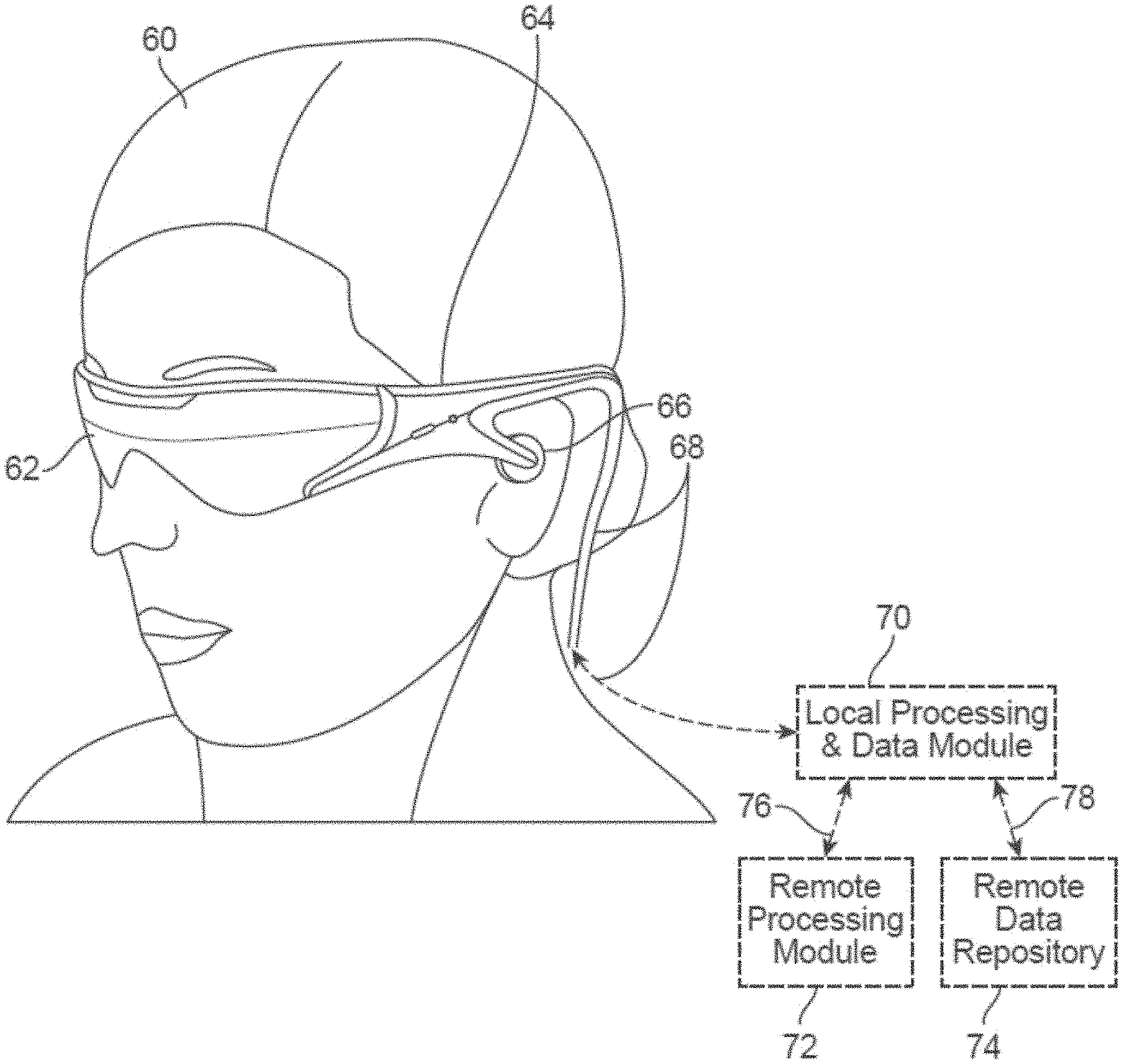
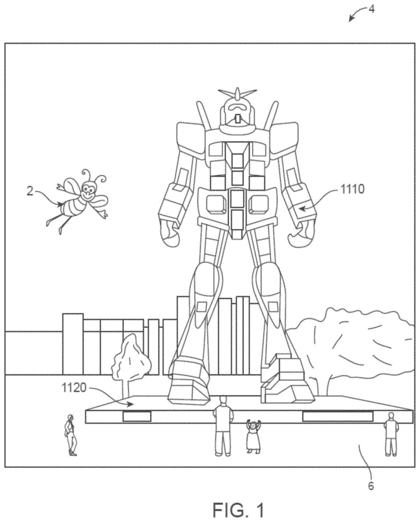
Modern computing and display technology has facilitated the development systems for so-called?virtual realities? “Modern computing and display technologies have facilitated the development of systems for so-called ‘virtual reality’ Digitally reproduced images, or portions of them, are displayed to the user in such a way that they appear to be real, or can be perceived to be so. Virtual reality (or ‘VR’) is a scenario where digital or virtual images are presented without any transparency with actual real-world input. A augmented reality (AR) scenario involves the presentation of digital image information to augment the visualization of the real world around the user. Referring to FIG. 1 shows an augmented-reality scene (4) where a user sees an actual park-like setting with people, trees and buildings in the back ground, as well as a concrete platform. The user of AR technology perceives, in addition to the items listed above, that he also’sees’ a robot statue (1110) standing on the real-world platform (1120), and a cartoon-like avatar character (2) flying by which seems to be bumble bee personified. A robot statue (1110) standing on the real-world platform (11120), as well as a cartoon avatar character (2), which appears to personify a bumblebee, are all perceived by the user of the AR technology, even though they do not exist. It turns out that the human visual system is complex. Producing a VR/AR technology that allows for a rich, comfortable presentation of virtual images amongst real or virtual imagery is challenging.
There are many challenges to overcome when presenting 3D content to an AR user. The main idea behind presenting 3D virtual content to users is creating the illusion of depth. It may be desirable to have some virtual content closer to the user and other virtual content appearing from a distance. To achieve 3D perception the AR system must be configured so that virtual content is delivered at different focal planes in relation to the user.
In order for a 3D screen to give a real sense of depth and, more specifically, to simulate the sensation of surface depth it is important that each point of the visual field of the display generates the accommodative reaction corresponding to the virtual depth of the point. The human visual system can experience an accommodation conflict if the accommodative responses to display points do not match the virtual depths as determined by binocular depth clues of stereopsis and convergence. This may result in unstable images, eye strain and headaches.
There is therefore a need to improve technologies in order to implement 3D displays which resolves these problems and others of the conventional approach. The systems and techniques described in this document are designed to work with the visual configurations of the average human to overcome these challenges.
Embodiments” of the present invention relate to devices, methods and systems that facilitate virtual reality or augmented reality interactions for one or several users.
Accordingly, additional embodiments provide improved approaches to implement deposition and imprinting imprint material onto a substrate to create patterns for implementing Diffraction. These methods allow for a very precise distribution, deposition and/or pattern formation on any number of substrates surfaces. In some embodiments, imprint material is deposited onto a substrate using patterned distribution of imprinting materials (e.g. patterned inkjet). The use of patterned inkjet distribution allows for a very precise control over the volume of materials to be deposited. This approach can also be used to create a more uniform, smaller base layer underneath a grating surface.
In some embodiments, the template has a set of deeper depth features along with a set of shallower depth features. In order to deposit imprint material onto an imprint recipient, a higher volume is used in conjunction with deeper depth structures. A relatively smaller volume of imprint material is also deposited with shallower depths of the template. This allows for simultaneous deposition of material thicknesses to form the various features onto the imprint recipient. This method can be used to create non-uniform distributions for structures that have different depths or feature parameters. For example, when the feature structures on the same substrate are of different thicknesses. This approach can be used to create spatially-distributed volumes of imprint materials that allow simultaneous imprinting of structures with variable depths and the same underlayer.
Some embodiments relate to a method to implement the simultaneous deposition multiple types of imprint material onto a substrate. It is possible to simultaneously deposit materials with optical properties on multiple areas of a substrate. This allows for the tuning of local areas that are associated with certain functions, such as acting as an in-coupling grating, orthogonal pupils expander (OPE), or exit pupil expansion (EPE). Different materials can be the same material with different optical properties, e.g. two variants of same material with different indices refractions. Or they could be two completely different materials. This technique allows for the selection of any optical property, such as opacity or absorption.
According to another embodiment, multiple-sided imprinting can be used to imprint different sides of an optical element. It is possible to imprint on the different sides of an element to achieve multiplexing through a volume of a base layer. This allows different eyepiece functions to be implemented without affecting the grating structure. One imprint can be produced on the side “A” using a first template. The substrate/imprint recipient is formed by a pattern with a material on side A. A second template can be used to create a second impression on the side “B”. The same substrate can be used to form a second pattern with a different material on side B. The sides A and B can have the exact same pattern or a different one, or they may contain the same material or a different type of material.
Additional embodiments relate to multi-layer substrate integration and/or separated/offset multi-layer substrate imprinting. In either/both approaches, an imprinted pattern can again be jetted onto and printed. A second substrate can be bonded (possibly using an airgap) to a first layer of adhesive, and then a jetting process is used to deposit the pattern onto it. Roll-to-roll processes can bond series-imprinted patterns in sequence. The multi-layer separation/offset substrate approach can be combined with or used instead of the multi-layer over imprinting approach. In multi-layer over imprinting, the first imprinting material is deposited onto a substrate, followed by a deposition of another imprinting material, which results in a composite multi-layer structure that has both a 1st imprinting material and 2nd imprinting material. In multi-layer separated/offset integration, a first substrate 1, and a second, offset substrate 2, may both be imprinted. Substrate 1 and 2 can then be sandwiched together and bonded with offset features that may also be imprinted. The air-gap can be created by using an imprinted spacer.
Accordingly, yet another embodiment is disclosed, an approach for implementing variable volume depositions of materials across the substrate. This may depend on an a priori understanding of surface non-uniformity. The surface non-uniformity on the substrate can result in undesirable parallelism and poor optical performance. Imprint material can be distributed evenly by using variable volume deposition, regardless of the topography of the substrate or its physical features. In situ metrology can be used to measure surface height using low coherence measurement probes or laser-based on-contact measurement. The imprint material dispense volume can be adjusted based on the measurement data in order to achieve a uniform layer. This embodiment of the invention can also address any types of non-uniformity, such as thickness variations and/or pits, peaks, or other anomalies associated with local positions of the substrate.
The detail description, figures, and claims describe “Additional and Other Objects, Features, and Advantages of the Invention.
According to some embodiments of the invention, a diffraction structure is employed that includes an underlayer/intermediate layer that resides between a waveguide substrate and a top grating surface. The top grating is made of a material with a refractive value that matches a 1st material, while the underlayer has a 2nd material matching a 2nd refractive value.
The advantage of this method is that by selecting the appropriate relative indices for the three layers, the structure can obtain a wider field of view and a greater range in incident light. This is because the minimum total internal reflection angle decreases as the index of refractive increases. The Diffraction efficiency can be improved, allowing for “brighter” light outputs to the displays of image viewing devices. “Light outputs can be increased to display(s) on image viewing devices.
A number of combinations are available, where an underlayer with one index is combined together with a top grating of another index and a substrate with a third index. By adjusting the relative values, a great deal of variation is provided in the dependence of diffraction on incidence angle. The presentation is of a layered waveguide that has different layers with refractive indexes. To illustrate functionality, a variety of combinations and permutations with associated performance data are shown. Benefits include an increased angle that provides a greater output angle for the grating, and therefore a larger field of view when using the eyepiece. The ability to counteract a normal decrease in diffraction with angle is also functionally beneficial.
Display Systems according to some Embodiments
This section of the disclosure describes examples of display systems that can be used with the improved diffraction structures of the invention.
Click here to view the patent on Google Patents.
Leave a Reply