
Invented by Oh-Kyong Kwon, Samsung Display Co Ltd
LED displays are known for their superior image quality, energy efficiency, and durability compared to traditional display technologies. They offer vibrant colors, high contrast ratios, and wide viewing angles, making them ideal for applications such as televisions, smartphones, tablets, and digital signage. The market for LED displays is driven by the growing popularity of high-definition content and the need for visually appealing displays in various sectors.
The display panel market, on the other hand, encompasses a wide range of technologies such as LCD (Liquid Crystal Display), OLED (Organic Light Emitting Diode), and MicroLED. LCD panels have dominated the market for several years due to their cost-effectiveness and widespread adoption. However, OLED panels are gaining traction due to their superior image quality, flexibility, and thin form factor. OLED panels are used in high-end smartphones, televisions, and wearable devices, and their market share is expected to increase in the coming years.
MicroLED, a relatively new technology, is also gaining attention in the display panel market. MicroLED panels offer several advantages such as high brightness, low power consumption, and self-emissive pixels, which eliminate the need for backlighting. Although MicroLED panels are currently expensive to produce, advancements in manufacturing processes are expected to drive down costs and increase their adoption in the future.
The driving method for LED and display panels plays a crucial role in their performance and efficiency. Various driving methods, such as passive matrix and active matrix, are used to control the individual pixels in a display panel. Active matrix driving methods, such as Thin-Film Transistor (TFT) technology, offer faster response times, higher resolutions, and better image quality compared to passive matrix methods. The market for driving methods is driven by the demand for high-resolution displays and the need for efficient power management.
In terms of geographical regions, Asia Pacific dominates the market for LED displays, display panels, and driving methods. The region is home to several major display panel manufacturers, such as Samsung, LG, and BOE, who are continuously investing in research and development to enhance their product offerings. North America and Europe also contribute significantly to the market, driven by the presence of major consumer electronics companies and the growing demand for advanced display technologies.
In conclusion, the market for Light Emitting Display, Display Panel, and Driving Method Thereof is witnessing robust growth due to the increasing demand for high-quality displays in various industries. LED displays, OLED panels, and MicroLED panels are gaining popularity due to their superior image quality, energy efficiency, and flexibility. The driving method for these displays is also evolving to meet the demands of high-resolution content and efficient power management. With advancements in technology and increasing investments in research and development, the market is expected to continue its growth trajectory in the coming years.
The Samsung Display Co Ltd invention works as follows
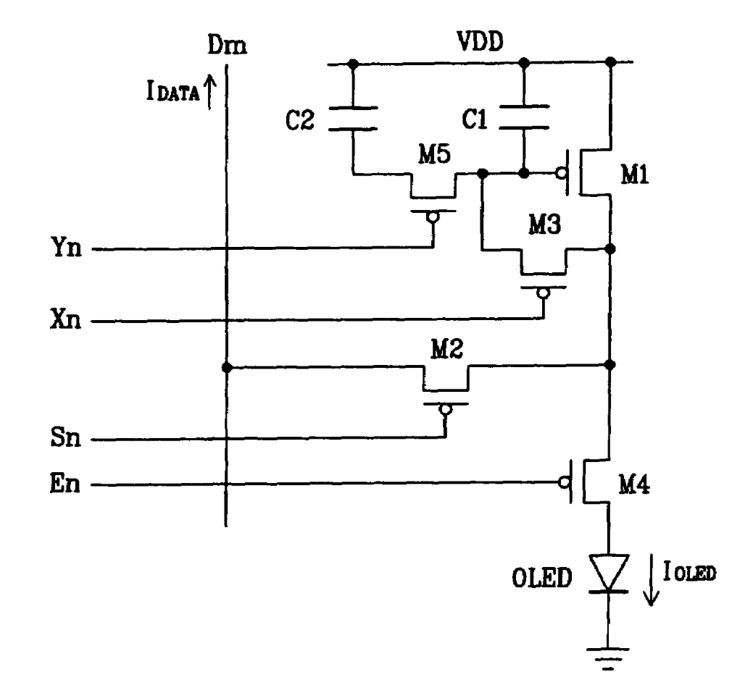
A light-emitting display that compensates for threshold voltage of transistors or mobility, and charges a dataline fully. On a pixel-circuit of an organic EL screen, a transistor and the first to third switches are formed. The transistor provides a driving voltage for an organic EL (OLED). The transistor is connected to the first switch diode. First storage unit stores first voltage that corresponds to threshold voltage of transistor. In response to the select signal, a second switch transmits data current. A second storage unit is used to store a second voltage that corresponds to the data current. Third switch transmits driving current to OLED. “A third voltage is determined by coupling the first and the second storage units, which is then applied to a transistor in order to supply the driving power to the OLED.
Background for Light emitting Display, Display Panel, and Driving Method Thereof
(a ) Field of the Invention
The present invention is a light-emitting display, display panel and driving method. The present invention is more specifically a display that uses an organic electroluminescent material (EL).
(b). Description of the Related Art”.
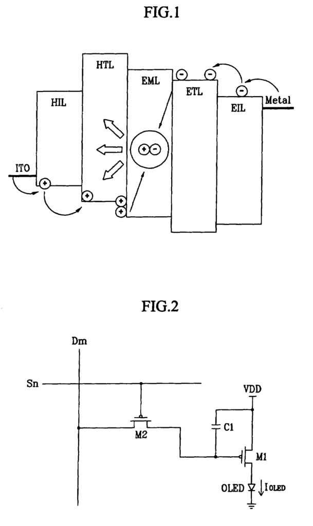
The active matrix method uses metal oxide semiconductor field-effect transistors or thin film transistors to drive the organic emitting cell. The passive matrix method crosses cathodes with anodes, and drives lines selectively. The active matrix method uses a TFT to maintain a voltage according to capacitance by connecting a capacitor to each ITO pixel. According to the signal forms provided for maintaining a capacitance, active matrix is classified as either a voltage or current programming method.
The voltage programming and current programming methods of organic EL displays will be described. “Referring to FIGS.
In order to operate the above-configured pixels, a data voltage is applied to transistor M1’s gate when transistor M2 turns on in response to a select line applied to its gate.” In this case, transistor M2 is turned on according to a select signal applied to the gate of switching transistor M2, and a data voltage from the data line Dm is applied to the gate of transistor M1.
Equation 1 gives the current flowing to the OLED in this case.
I\nOLED\n=\n?\n2\n?\n(\nV\nGS\n-\nV\nTH\n)\n2\n=\n?\n2\n?\n(\nV\nDD\n-\nV\nDATA\n-\n?\nV\nTH\n?\n)\n2\nEquation\n?\n?\n1
where VGS is the voltage between the source of the transistor M1 and its gate, VTH is the threshold voltage on transistor M1,? is a constant and? is the voltage at the transistor M1’s gate.” “where IOLED is the current flowing to the OLED, VGS is a voltage between the source and gate of transistor M1, VTH is a threshold voltage at transistor M1, and?
According to FIG., the OLED emits light according to its current supply, as shown in Equation 1. 2. The applied voltage is multi-staged within a range of values that has been pre-determined to represent gray.
However the conventional pixel system using the voltage programming method is prone to a problem, in that it’s difficult to achieve high gray due the deviations in a threshold voltage (VTH) of a transistor and the deviations in electron mobility as a result of non-uniformity during an assembly process. In the case of driving the TFT in a pixel at 3 volts (3V), the voltages to the gate TFT are supplied for every interval of 12mV (=3V/256), so that 8-bit grays (256) can be represented. If the threshold voltage caused by non-uniformity in the assembly process is deviated, it becomes difficult to represent high grey. It is also difficult to represent high gray because the value of Equation 1 changes due to the deviation in mobility. The high gray is even more difficult to depict because the value?
The current programming method, assuming the current source to supply the current to the pixels circuit is uniform across the entire panel, can achieve uniform display characteristics even if a driving transistor within each pixel does not have uniform voltage-current characteristics.
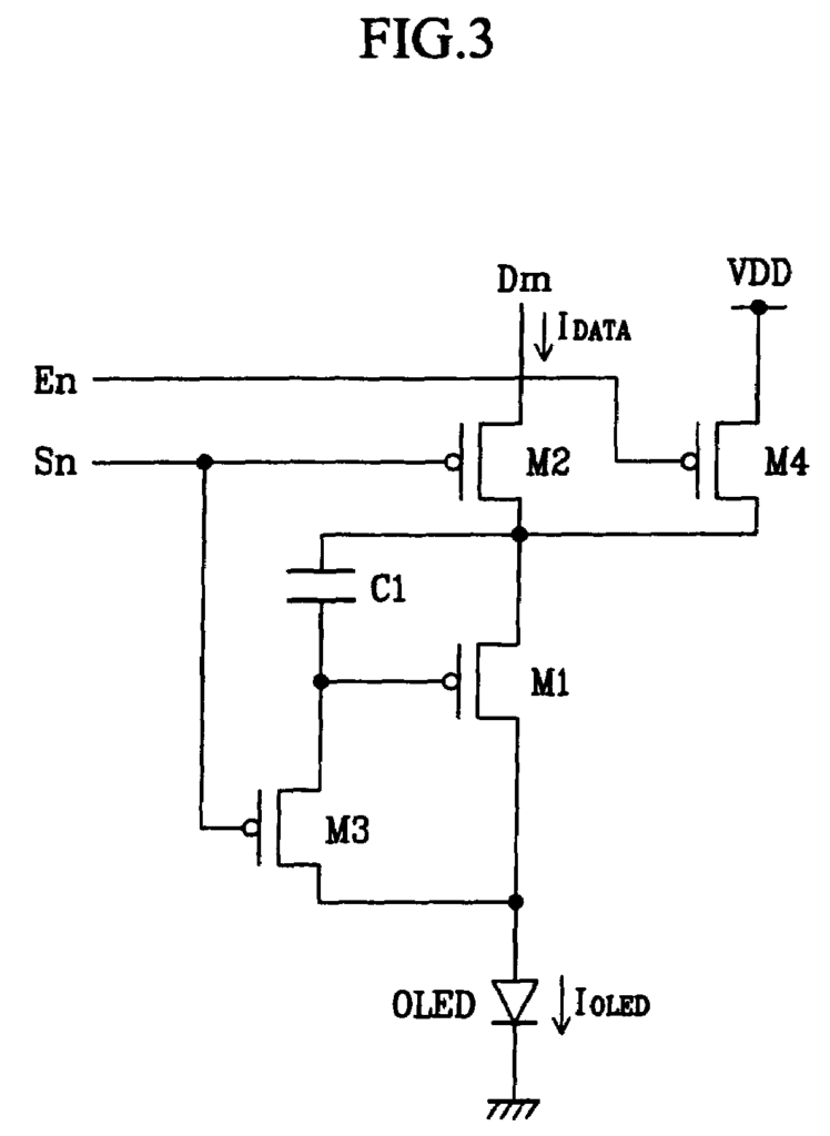
First, the transistor M1 is diode connected when the scan line Sn turns on transistors M2 or M3. The voltage matching the data current IDATA of data line Dm in capacitor C1 is then stored. The select signal from scanline Sn is then raised to high level, enabling transistor M4. Next, power is provided by voltage VDD and the current matching the voltage stored in C1 flows into the OLED for light emission. The current flowing to OLED in this case is shown below.
I\nOLED\n=\n?\n2\n?\n(\nV\nGS\n-\nV\nTH\n)\n2\n=\nI\nDATA\nEquation\n?\n?\n2
where VGS represents a voltage between transistor M1’s source and gate, VTH is the threshold voltage of transistor M1,? is a constant.” “where? is a constant.
As shown in Equation 2, because the data current IDATA flowing through the OLED and the current IOLED flowing into the OLED are the same, uniform characteristics can only be achieved when the programming current is uniformly applied to the entire panel. Since current IOLED flowing into the OLED has a very fine current, it is difficult to control the pixel circuit using fine current IDATA. Assuming, for example, that the data-line load capacitance is 30 pF it takes several milliseconds to charge the data-line load with a data current of up to several hundred nA. The charging time becomes insufficient when the line time is several tens microseconds.
According to the present invention, a light-emitting display is provided that compensates for the threshold voltage of the transistors or the electron mobility and charges the data line sufficiently.
The pixel circuit includes: a light-emitting element for emitting light corresponding to the applied current; a first transistor, having first and second main electrodes and a control electrode, for supplying a driving current for the light-emitting element; a first switch for diode-connecting the 1st transistor in response to a 2nd control signal; a storage unit for storing a voltage corresponding to a threshold voltage of the 1st transistor in response a 3 The pixel circuit comprises: a light-emitting element that emits light in accordance with the applied current, a transistor having first and secondary main electrodes, and a control element, to supply a driving voltage for the light-emitting element, a diode switch to connect the transistor in response a a signal, a storage unit to store a voltage first corresponding a threshold voltage for the transistor in response a signal, a switch to transmit a data signal in response a scan line in response a select line, a scan line, a a a a a a a a a a a a a a a, a a a a a a a a a a a a a a the The first transistor is supplied with a third voltage by coupling the first storage unit and the second storage unit respectively. In order, the second control signal, select signal, and third control signal are enabled. A fourth switch is also included in the pixel circuit, which is activated by the second control signal and connected to a control electrolyte of the first transistor. A first capacitor is coupled between the control and first main electrodes of the transistor to form the second storage unit. The first storage unit consists of parallel coupling a second capacitance coupled between the main electrode of the transistor’s first transistor and the second end of the switch. The second control is the select from the scanline, and the fourth switches responds to the disable interval. The first control signals include a select from the previous scanline and a current scanline select. The first switch has a second transistor that diode connects the first transistor when the select from the previous scan is received, and a 3rd transistor to diode connect the first transistor when the select from the current scan is received. The second control signals include a select from the previous scan lines and the third control signals. A fifth switch is also included in the pixel circuit, which is coupled parallel to the 4th switch. The fourth and fifth switches are turned on respectively in response to the scan line select signal and the third control signals.
Click here to view the patent on Google Patents.
Leave a Reply