Invented by Byung Hee Kim, Samsung Display Co Ltd
One of the key factors contributing to the growth of the OLED market is the rising popularity of smartphones and other portable electronic devices. OLED displays are widely used in smartphones due to their ability to produce vibrant colors and deep blacks, resulting in an immersive visual experience for users. Additionally, the flexibility of OLED technology allows for the creation of curved and flexible displays, which further enhances the design possibilities for smartphones and wearable devices.
Another significant driver of the OLED market is the increasing adoption of OLED televisions. OLED TVs offer superior contrast ratios and color accuracy compared to LCD TVs, making them highly sought after by consumers who prioritize picture quality. The demand for OLED TVs is expected to surge in the coming years as prices continue to decline, making them more accessible to a wider range of consumers.
The automotive industry is also a promising market for OLED displays. OLED technology enables the creation of thin and curved displays that can be seamlessly integrated into the interior design of vehicles. OLED displays are used for instrument clusters, infotainment systems, and even external lighting, providing a visually appealing and intuitive user interface for drivers and passengers.
In terms of fabrication methods, there are several techniques employed in the manufacturing of OLED displays. One commonly used method is vacuum thermal evaporation, where organic materials are heated in a vacuum chamber and then deposited onto a substrate to form the OLED layers. This method allows for precise control over the thickness and uniformity of the organic layers, resulting in high-quality displays.
Another method is inkjet printing, which offers advantages such as lower manufacturing costs and the ability to print OLED layers directly onto flexible substrates. Inkjet printing also allows for the deposition of multiple colors simultaneously, enabling the creation of full-color displays in a single pass. However, challenges such as material compatibility and scalability need to be addressed for inkjet printing to become a mainstream fabrication method for OLED displays.
Overall, the market for OLED devices and the methods used to fabricate them are experiencing significant growth and innovation. As consumer demand for high-quality displays continues to rise, OLED technology is poised to dominate the market, offering superior visual experiences across various applications. With ongoing advancements in fabrication techniques, OLED displays are expected to become even more affordable and versatile, further fueling their adoption in smartphones, televisions, automotive displays, and other emerging markets.
The Samsung Display Co Ltd invention works as follows
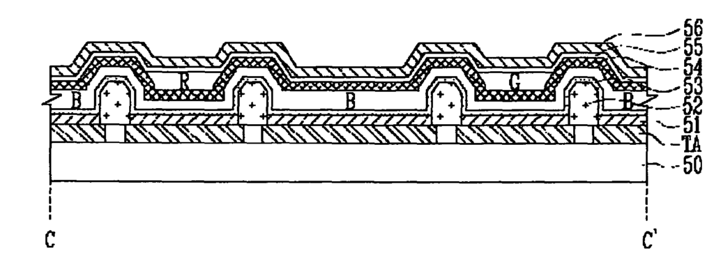
In an organic display with light-emitting pixels and the fabrication method thereof, a change in the layout of each pixel is made to increase the luminous efficiency of a pixel region that has a low level. At least one pixel of the organic light emitting displays contains sub pixels with a variety of colors. Over the entire surface of a pixels region, a first sub-pixel emission layer is formed. The first sub pixel layer is followed by at least two other sub pixel layers that have a closed curvature. In order to improve life expectancy and aperture ratio, the layout of pixels is altered to increase the area of a sub-pixel region with low luminous efficacy. During the formation of an emissions layer, masks are reduced. In this way, the likelihood of misalignment decreases, which maximizes resolution, improves yield and reduces manufacturing costs.
Background for Organic Light Emitting Display Device and Method for Fabricating the Same
1. “1.
The present invention is a method of fabricating an organic light-emitting display. The present invention is more specifically an organic light-emitting display and a fabrication method, wherein the layout of pixels is altered to increase the luminous efficiency in a pixel region with low luminosity.
2. “2.
Flat panel displays have recently been developed that can reduce weight and volume – two disadvantages of the cathode tube (CRT). Flat panel displays are liquid crystal displays, field emission displays, plasma display panels and organic light emitting devices.
The next generation of flat-plate displays will be light emitting displays. They have a greater temperature range of use, are more resistant to vibration or shock, have a larger viewing angle, and have a faster response time.
Such light-emitting displays include organic light-emitting displays using an organic diode, and inorganic display light-emitting displays using an inorganic diode. The organic light-emitting diode consists of an anode and cathode electrodes, as well as an organic emission layer that is disposed between them. This organic emission layer emits light using a combination electrons and hole. Inorganic light-emitting diodes include an inorganic layer of light emitting material composed of a PN Junction semiconductor.
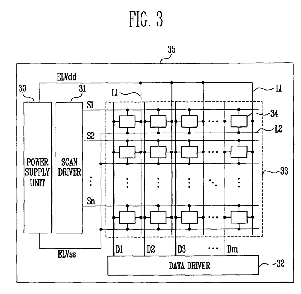
The organic light-emitting display is composed of red (R), blue (B), and green (G) materials deposited in sub-pixel regions on at least one pixel area on a substrate. These sub-pixel regions emit light when a thin film semiconductor on the substrate is driven. Red (R), Green (G), Blue (B) sub-pixel regions are disposed in different locations to achieve a full-color display. This is because the human eye can only recognize colors that are based on three primary colours.
Previous displays were plagued with several disadvantages. It is hard to produce displays with a longer life expectancy because there are limitations to the manufacturing of sub-pixel regions of a particular color. A laser thermal transfer technique has been developed to solve this problem. However, it is limited by its high cost and difficulty in improving the quality.
In some previous displays, the different sub-pixels must be patterned by using different colors of masks. In this case there is a misalignment problem, which results in a deterioration of the resolution. A more precise patterning method is also required.
It is the object of this invention to provide a organic light-emitting display, and a fabrication method, in which a layout is altered to increase the life of a pixel with low luminous efficiency.
The present invention also aims to reduce the number of masks required for the formation of an emission layer.
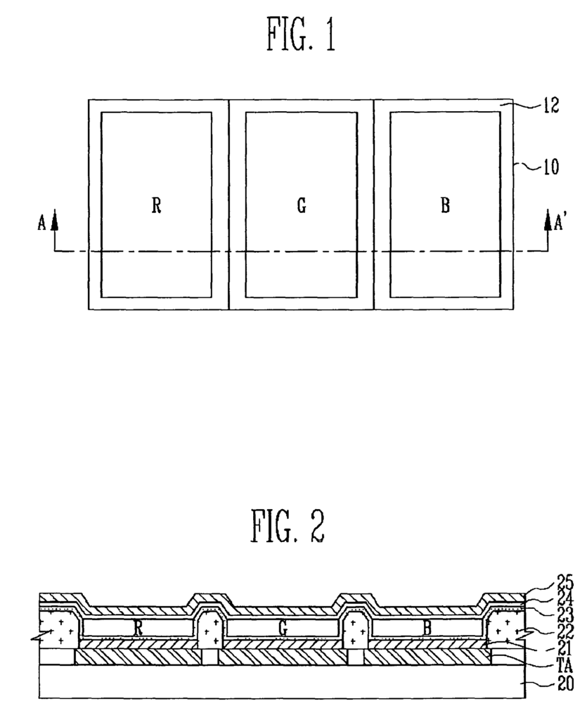
The foregoing or other aspects of the invention are achieved by providing a organic light emitting screen comprising atleast one pixel, including sub pixels with a plurality colors. This display comprises: a sub-pixel layer that covers the entire surface of the pixel region and at least two sub-pixel layers that form a closed curvature at the sub-pixel layer.
Preferred, the first sub-pixel emission layer should be formed in a color of blue. The first sub-pixel emission layer has a larger forming area than the second sub-pixel emission layers. The organic light emitting displays is more preferably further comprised of an electron blocking film formed over the entire surface between the first sub-pixel emission layer, and the at the least two second sub-pixel emission layers.
According to another aspect, an organic light-emitting display includes at least one pixel with sub pixels that have a variety of colors. It also comprises: At least two sub-pixel emission levels formed on a region of a pixel so as not overlap; and a sub-pixel emission layer over the entire surface of the region of the pixel so as to include at least the two sub-pixel emission.
The second sub-pixel emission layer should be formed in a way that it has a blue colour.” The second sub-pixel emission layer has a larger forming area than the first two sub-pixel emission layers. The organic light emitting displays are further preferably provided with a hole-blocking layer that is formed on the entire surface between the first and second sub pixel layers.
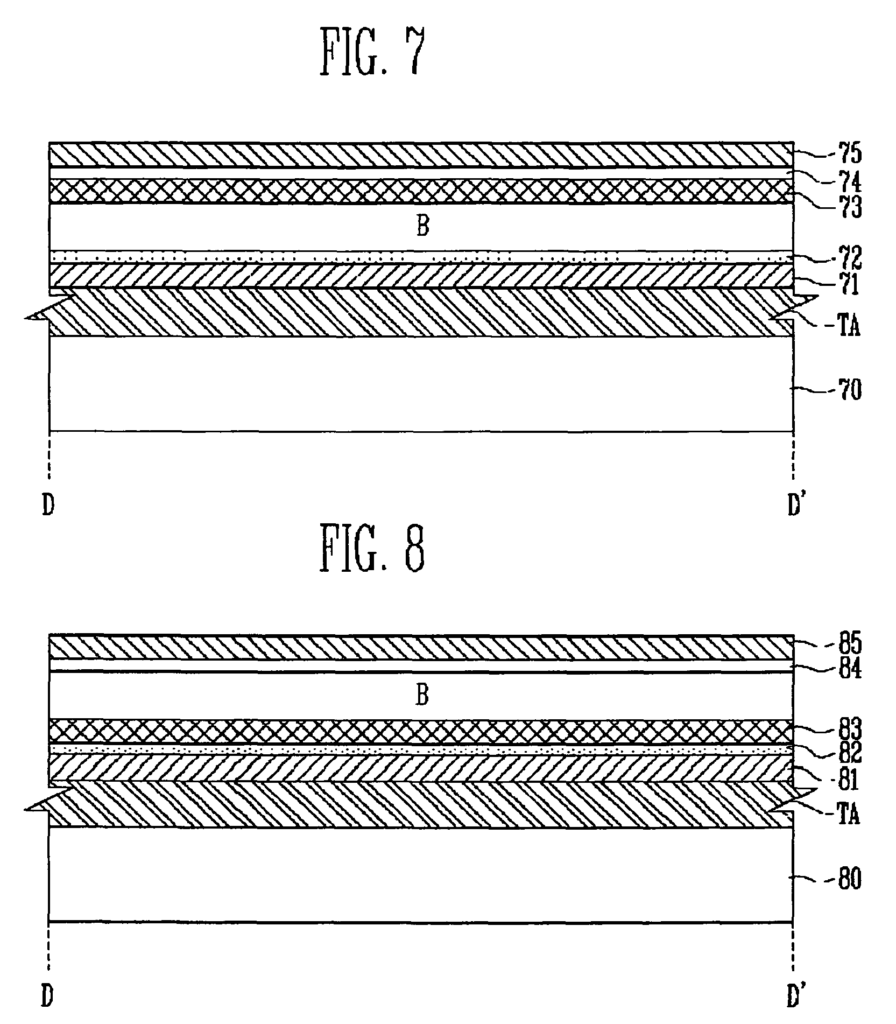
According to a further feature of the invention, an organic display includes at least one pixel with sub pixels that have multiple colors. It also comprises: first electrodes, which are included in each sub-pixel and are formed on a region of a substrate, a sub-pixel emission film formed over the entire surface of the pixel region, a second sub-pixel emission film formed so that it has a closed curvature, a third sub-pixel emission film formed so that it has a closed curvature at a
The first sub-pixel emission layer should be formed in a way that it has a blue colour.” The first sub-pixel emission layer’s forming area, excluding the forming areas for the second sub-pixel emission layer and the third sub-pixel emission, must be greater than the forming area of each second sub pixel emissions layer.
The organic light emitting displays further comprise an electron blocking layers formed over the entire surface between the first sub-pixel emission layer and the second sub-pixel emission layer, and the electron block layer is formed from Ir(ppz3)3.
The second and third sub-pixel emission layers are formed in a red and green color, respectively. The second and fourth sub pixel emissions layers in this embodiment are colored red and green, respectively. In addition, the first and second sub pixel layers are arranged into a stripe and delta pattern.
According to an additional aspect, an organic light-emitting display includes at least one subpixel having a variety of colors. The at least one subpixel comprises: first electrodes formed on a region of an pixel area on a first electrode, a second subpixel emission on a different region of the same pixel area on the second electrode, a third subpixel emission formed over the entire surface of an pixel on the third electrode, and the second and third subpixel emission on the second and third subpixel emission layers
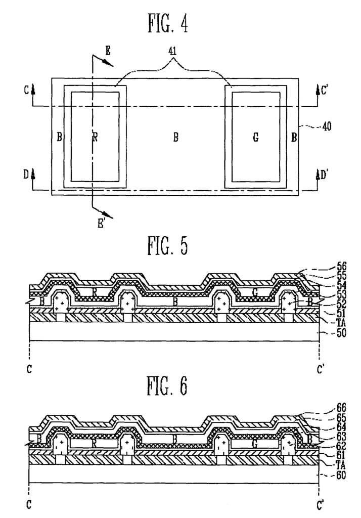
The third sub-pixel emission layer should be formed in a blue colour. Its forming area, excluding the forming areas of first and the second sub-pixel emission layers, must be greater than each of these first and the second sub-pixel emission layers.
Click here to view the patent on Google Patents.

Leave a Reply